SEMICONDUCTOR AND OPTOELECTRONIC METHODS and DEVICES

a technology of optoelectronic and semiconductor devices, applied in semiconductor devices, television systems, radio frequency controlled devices, etc., can solve the problems of less efficient mixing of red, blue and green colors to form white light, much more expensive than pcleds, and rgb-led is still much more expensive than a pcled solution

Active Publication Date: 2016-03-03
MONOLITHIC 3D
View PDF10 Cites 50 Cited by
  • Summary
  • Abstract
  • Description
  • Claims
  • Application Information

AI Technical Summary

Benefits of technology

[0052]In another aspect, a method for enabling 3D viewing of objects in an image through actual physical distances of individual objects to the viewer displayed separately on a display screen actuated by a fast motor.

Problems solved by technology

While RGB LEDs are more energy-efficient than pcLEDs, they are less efficient in mixing red, blue and green colors to form white light.
They also are much more costly than pcLEDs.
While this solves light mixing problems, this RGB-LED is still much more costly than a pcLED solution since three LEDs for red, blue, and green color need to be packaged.
However, red LEDs are not efficient when constructed with GaN-based material systems, and that hampers usefulness of this implementation.
It is not possible to deposit defect-free AlInGaP / InGaP for red LEDs on the same substrate as GaN based blue and green LEDs, due to a mismatch in thermal expansion co-efficient between the various material systems.
Unfortunately, this bonding process requires 600° C. temperatures, causing issues with mismatch of thermal expansion co-efficients and cracking.
Bonding is done at the die level after dicing, which is more costly than a wafer-based approach.
This method has several issues for constructing a RGB LED stack.
First, it is difficult to manufacture a lift-off with a temporary carrier of red LEDs for producing a RGB LED stack, especially for substrates larger than 2 inch.
Scaling this process to 4 inch wafers and bigger is difficult.
Second, it is very difficult to perform the bonding of ITO to semiconductor materials of a LED layer at reasonable temperatures, as described in the patent application Ser. No. 12 / 130,824.
Since the area consumed by the sensing circuits is high, the photodetector cannot see the entire incident light, and image capture is not as efficient.
However, pixel size is reaching the 1 μm range, and successfully processing TSVs in the 1 μm range or below is very difficult.
This is due to alignment issues while bonding.
Unfortunately, transistor process temperatures reach 600° C. or more.
This is not ideal for transistors (that require a higher thermal budget) and photodetectors (that may prefer a lower thermal budget).
While lift-off layer transfer schemes are viable for transmittive displays, they are frequently not used for semiconductor manufacturing due to yield issues.
However, it is not easy to utilize other layer transfer schemes for making transistors in microdisplays.
Unfortunately, hydrogen is implanted through the gate oxide of transferred transistors in the process, and this degrades performance.
Process temperatures are as high as 600° C. in this paper, and this requires costly glass substrates.
There are a few issues with standard multi junction solar cells.
Therefore, the choice of materials used to build junctions for multi-junction solar cells is limited.
As a result, most multi-junction solar cells commercially available today cannot capture the full solar spectrum.
Furthermore, multi-junction solar cells today suffer from high cost of the substrate above which multiple junctions are epitaxially grown.
The process uses two Germanium substrates, and is therefore expensive.
When that happens, cracking and defects can be produced due to mismatch of co-efficients of thermal expansion between various layers in the stack.
Furthermore, semiconductor layers are bonded together, and the quality of this bond not as good as oxide-to-oxide bonding, especially for lower process temperatures.
On the other hand, in a CMOS sensor, the photodiodes in each cell have to share space with the control and readout circuits adjacent to them, and so their size and light sensitivity are therefore limited.
The main issue with CCD technology is this sequential shifting of image information from cell to cell is slow and limits the speed and cell density of CCD image sensors.
The concept of HDR however, is not new.
The issue with this is that multiple exposures are performed over some period of time, and if there is movement of the camera or target during the time of the exposures, the final HDR image will reflect this by loss of sharpness.
Moreover, multiple images may lead to large data in storage devices.
Other methods use software algorithms to extract HDR information from a single exposure, but as they can only process information that is recordable by the sensor, there is a permanent loss of some details.
However, wires (interconnects) that connect together transistors degrade in performance with “scaling”.

Method used


Image

  • SEMICONDUCTOR AND OPTOELECTRONIC METHODS and DEVICES
  • SEMICONDUCTOR AND OPTOELECTRONIC METHODS and DEVICES
  • SEMICONDUCTOR AND OPTOELECTRONIC METHODS and DEVICES

Examples


Embodiment Construction

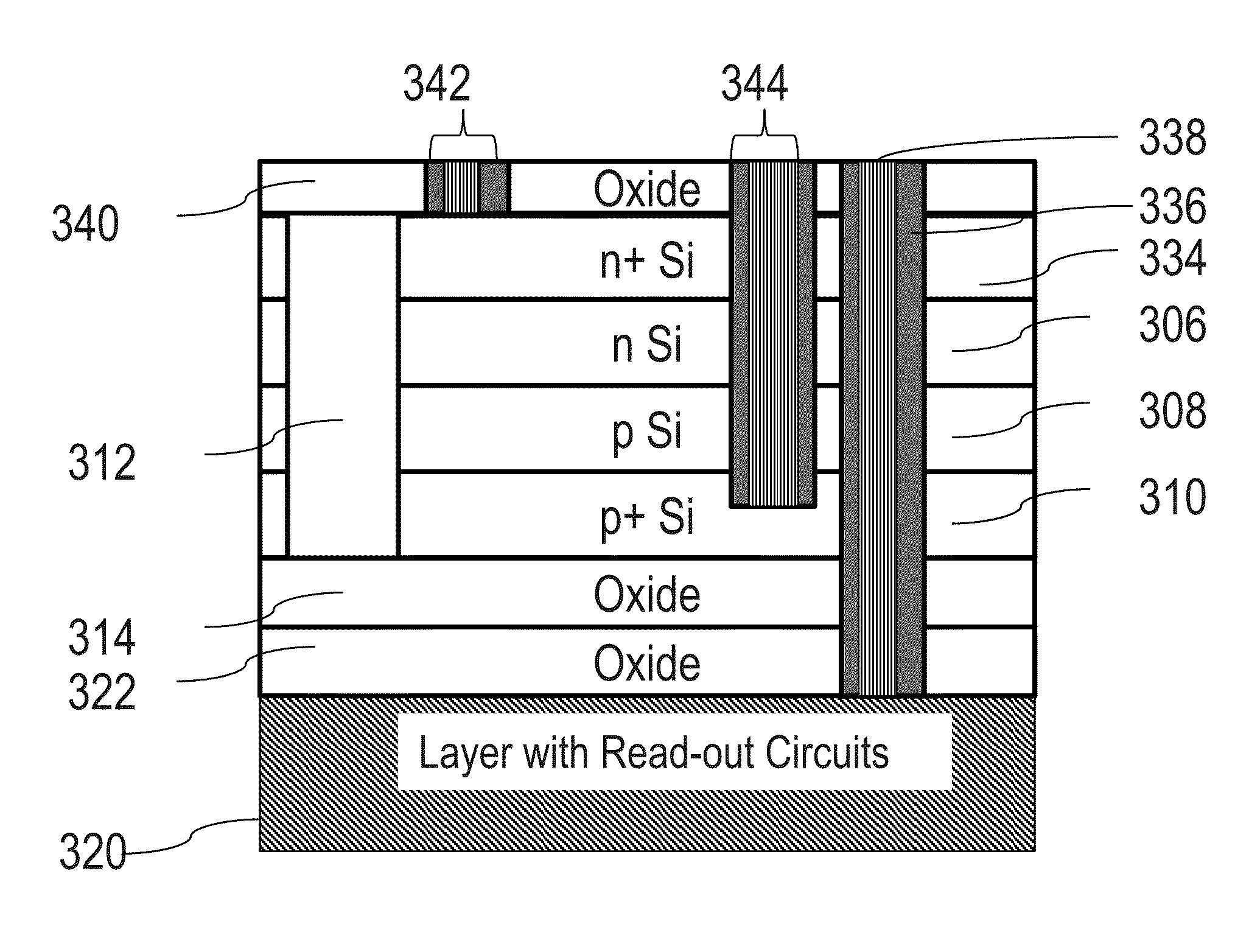
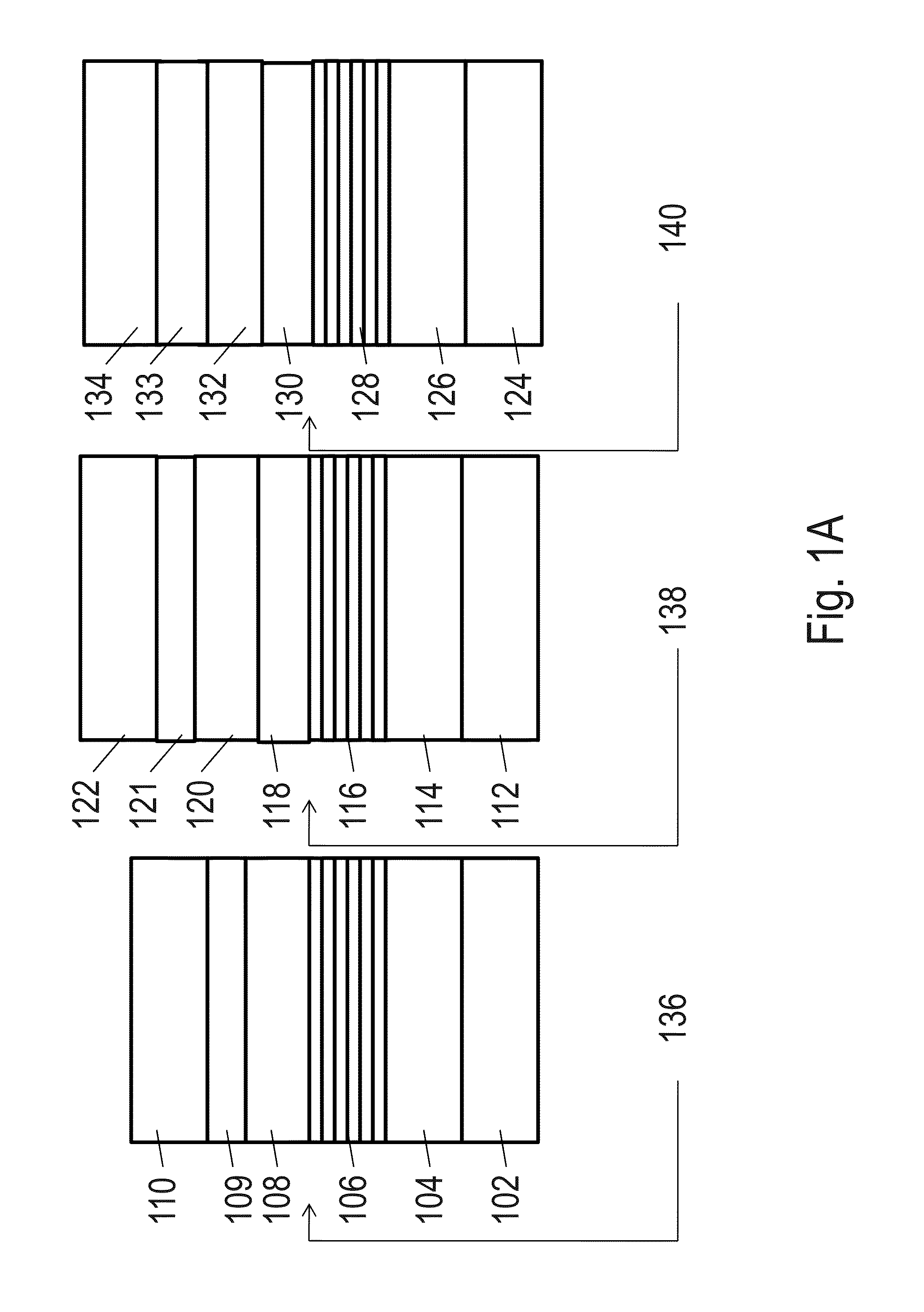
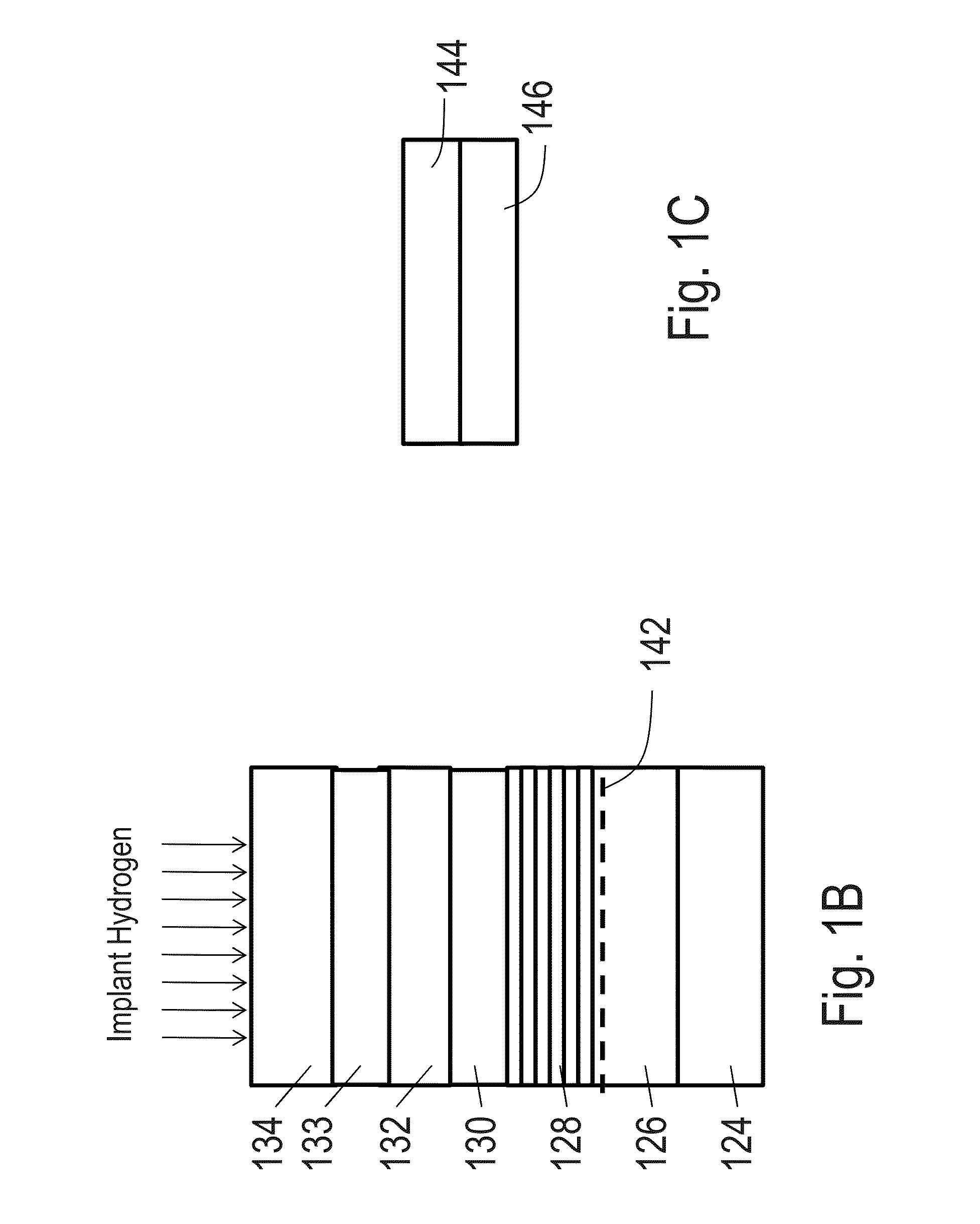
[0097]Embodiments of the present invention are now described with reference to FIGS. 1-25, it being appreciated that the figures illustrate the subject matter not to scale or to measure.

NuLED Technology:

[0098]FIG. 1A-S illustrate an embodiment of this invention where Red, Blue, and Green LEDs are stacked on top of each other with smart layer transfer techniques. A smart layer transfer may be defined as one or more of the following processes:[0099]Ion-cut, variations of which are referred to as smart-cut, nano-cleave and smart-cleave: Further information on ion-cut technology is given in “Frontiers of silicon-on-insulator,” J. Appl. Phys. 93, 4955-4978 (2003) by G. K. Celler and S. Cristolovean (“Celler”) and also in “Mechanically induced Si layer transfer in hydrogen-implanted Si wafers,” Appl. Phys. Lett., vol. 76, pp. 2370-2372, 2000 by K. Henttinen, I. Suni, and S. S. Lau (“Hentinnen”).[0100]Porous silicon approaches such as ELTRAN: These are described in “Eltran, Novel SOI Wafer...


PUM


Abstract

A method for processing a semiconductor wafer, the method including: providing a semiconductor wafer including an image sensor pixels layer including a plurality of image sensor pixels, the layer overlaying a wafer substrate; and then bonding the semiconductor wafer to a carrier wafer; and then cutting off a substantial portion of the wafer substrate, and then processing the substantial portion of the wafer substrate for reuse.

Description

CROSS-REFERENCE OF RELATED APPLICATIONS[0001]This application is a continuation in part of U.S. patent application Ser. No. 13 / 274,161 filed on Oct. 14, 2011; and this application claims priority of U.S. patent application Ser. No. 12 / 904,103, now U.S. Pat. No. 8,163,581, the contents of all of the preceding are incorporated herein by reference.BACKGROUND OF THE INVENTION[0002](A) Field of the Invention[0003]This invention describes applications of monolithic 3D integration to various disciplines, including but not limited to, for example, light-emitting diodes, displays, image-sensors and solar cells.[0004](B) Discussion of Background Art[0005]Semiconductor and optoelectronic devices often require thin monocrystalline (or single-crystal) films deposited on a certain wafer. To enable this deposition, many techniques, generally referred to as layer transfer technologies, have been developed. These include:[0006]Ion-cut, variations of which are referred to as smart-cut, nano-cleave an...

Claims


Application Information

Patent Timeline
Patent Type & Authority Applications(United States)
IPC IPC(8): H01L27/146
CPCH01L27/14634H01L27/14687H01L27/1469H01L27/14632H01L27/14607H01L27/14685H04N5/232H01L21/70H04N5/225H01L25/0756H01L27/14623H01L27/14629H01L27/14647H01L33/382
Inventor OR-BACH, ZVISEKAR, DEEPAK, C.
Owner MONOLITHIC 3D
Why Eureka
Try Eureka