
Electric connection and method of manufacturing the same

a manufacturing method and technology of electric connection, applied in the direction of conductors, semiconductor/solid-state device details, semiconductors, etc., can solve the problems of reducing the reliability of contacts, affecting the service life of contacts, and damage to electronic components on the wafer, so as to achieve high ductility and thermal stability, low melting point, and high mobility

Active Publication Date: 2016-05-05
NAT CHENG KUNG UNIV
View PDF3 Cites 0 Cited by
  • Summary
  • Abstract
  • Description
  • Claims
  • Application Information

AI Technical Summary

Benefits of technology

The present invention aims to provide an electric connection with high ductility and thermal stability. To achieve this, we introduce gallium (Ga) and nickel (Ni) into a Cu-to-Cu connection to avoid conventional brittle intermetallic compound (IMC) formation during soldering. This addresses the reliability concerns associated with IMC formation. The relatively low melting point of Ga metal also allows for reliable interconnection formation at low temperatures and pressures.

Problems solved by technology

These complex procedures and precautions make the direct diffusion bonding a relatively costly and complicated process.
In addition, the required high pressure is not only costly, but may cause damages to the electronic components on the wafer.
However, solders are commonly composed of tin (Sn), which can readily react with the Cu metal as the substrates to produce a large fraction of brittle and electrical resistant intermetallic compound (IMC) formation in the contacts, thereby significantly reducing the reliability of the contacts.

Method used


Image

  • Electric connection and method of manufacturing the same
  • Electric connection and method of manufacturing the same
  • Electric connection and method of manufacturing the same

Examples


Embodiment Construction

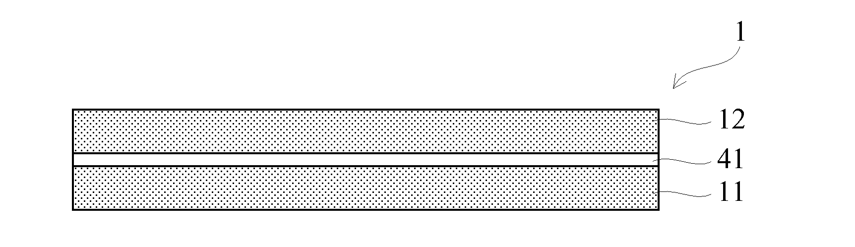
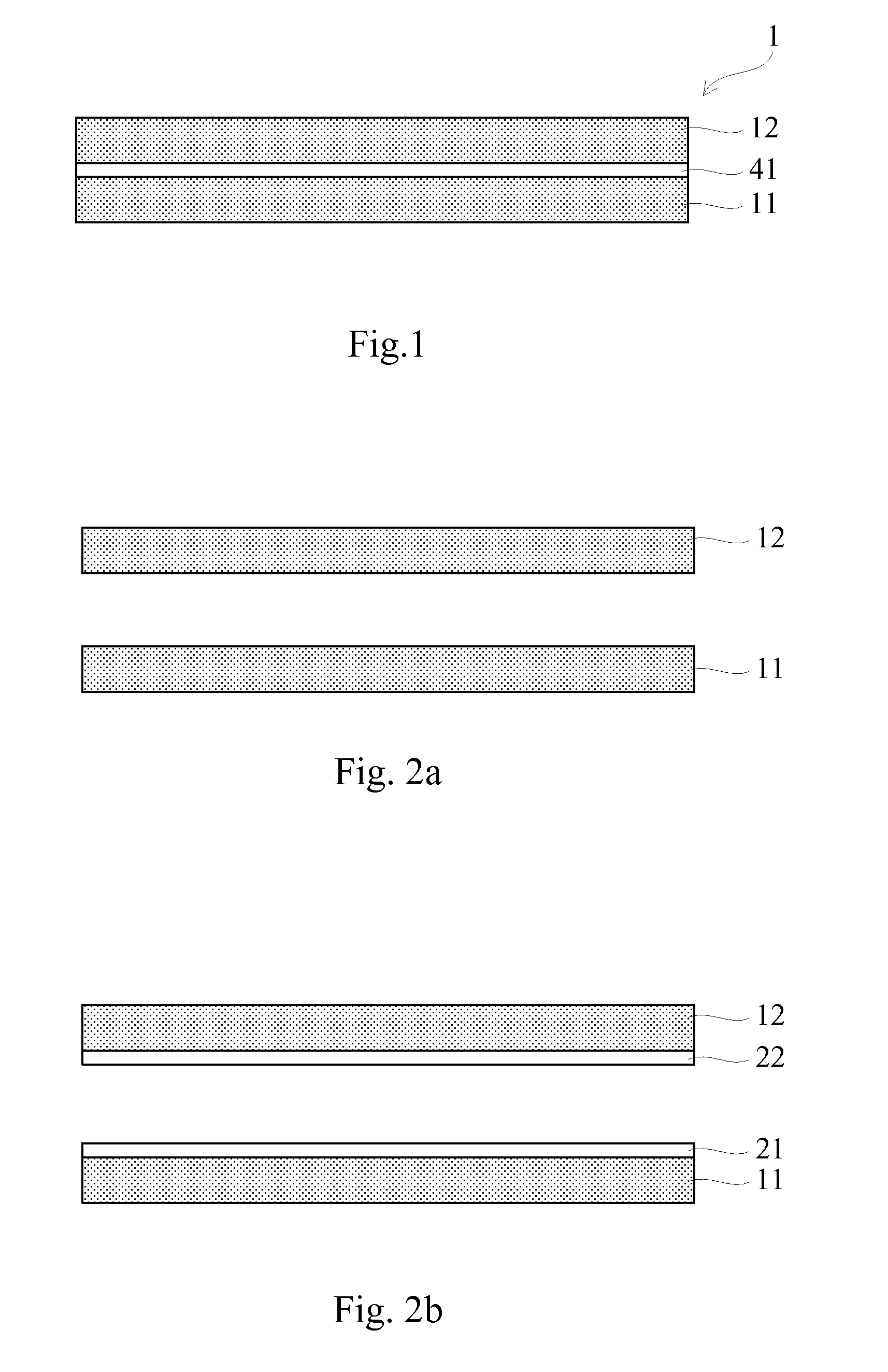
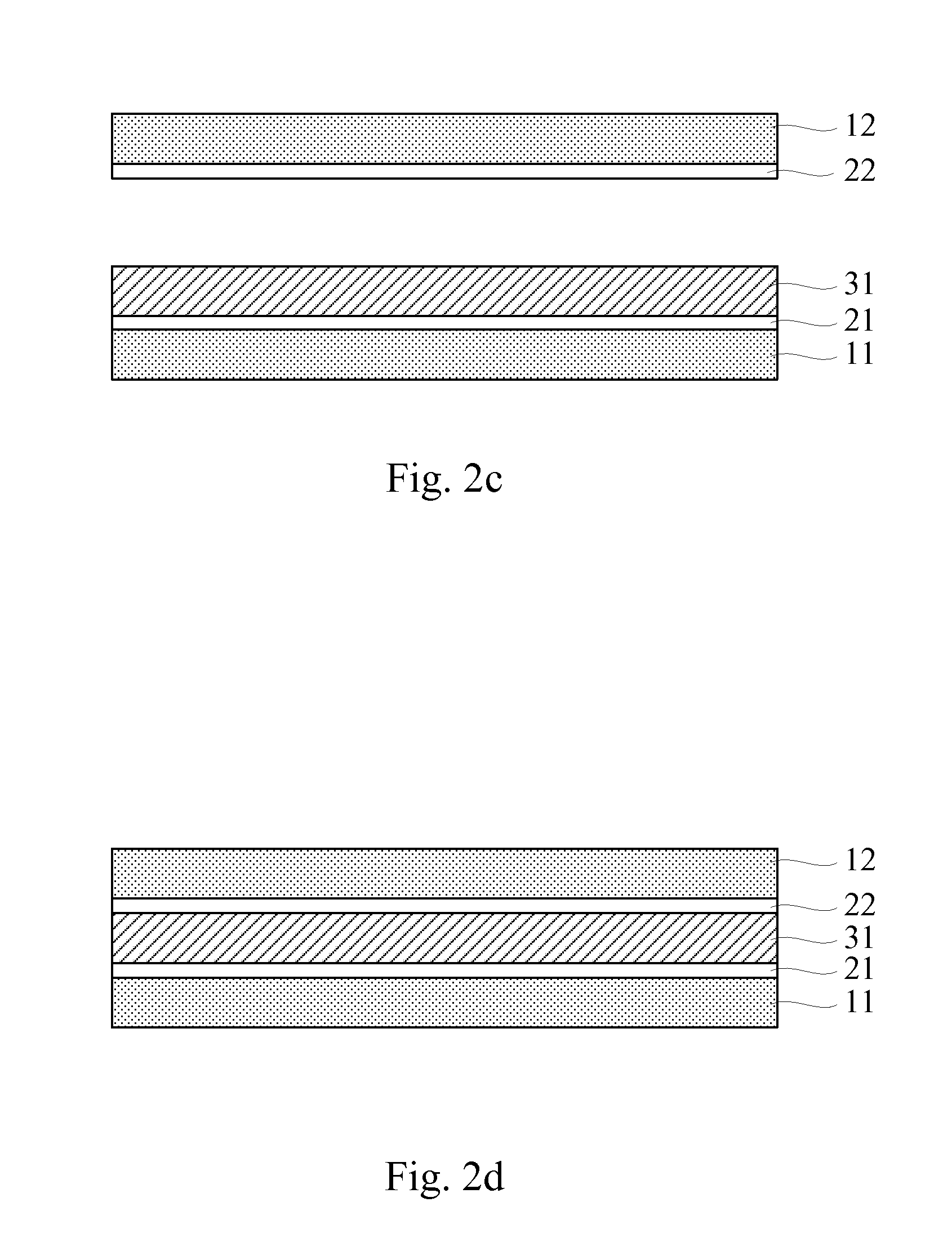
[0025]The structure and the technical means adopted by the present invention to achieve the above and other objectives can be best understood by referring to the following detailed description of the preferred embodiments. In addition, directional terms described by the present invention, such as upper, lower, front, back, left, right, inner, outer, side, etc., are only directions by referring to the accompanying drawings, and thus the directional terms are used to describe and understand the present invention, but the present invention is not limited thereto. Furthermore, if there is no specific description in the invention, singular terms such as “a”, “one”, and “the” include the plural number. For example, “a compound” or “at least one compound” may include a plurality of compounds, and the mixtures thereof. If there is no specific description in the invention, the “%” means “weight percentage (wt. %)”, and the numerical range (e.g. 10%˜11% of A) contains the upper and lower limi...


PUM

PropertyMeasurementUnit
melting pointaaaaaaaaaa
pressureaaaaaaaaaa
temperatureaaaaaaaaaa

Abstract

An electric connection is provided, and has a first copper (Cu) layer, a second Cu layer, and a composite metal layer disposed between the first Cu layer and the second Cu layer. The composite metal layer has 0.01 wt. %≦gallium (Ga)≦20 wt. %, 0.01 wt. %≦copper (Cu)≦50 wt. %, and 30 wt. %≦nickel (Ni)≦99.98 wt. %. Moreover, a method of manufacturing the electric connection is provided, and has the steps of: (1) providing a first Cu layer and a second Cu layer; (2) forming a first Ni layer on the first Cu layer; (3) forming a second Ni layer on the second Cu layer; (4) forming a Ga layer on the first Ni layer; and (5) keeping the second Ni layer in contact with the Ga layer and carrying out a thermo-compress bonding therebetween to form the electric connection.

Description

CROSS REFERENCE TO RELATED APPLICATIONS[0001]This application claims the benefit of priority of Taiwan Patent Application No. 103138070, filed on Nov. 3, 2014, the disclosure of which is incorporated herein by reference.FIELD OF THE INVENTION[0002]The present invention relates to an electric connection and a method of manufacturing the electric connection, and in particular relates to a copper-to-copper (Cu-to-Cu) electric connection.BACKGROUND OF THE INVENTION[0003]In recent years, the development trend of electronic semiconductors, miniaturization, high efficiency, low consumption and low cost are continuously pursued. Through Silicon Via (TSV) is to drill a via on a wafer or a chip by a laser, and then to fill the hole with a conductive material to form a conductive path, thereby vertically connecting the upper and lower surfaces of the wafer, enabling the stacking multiple chips. This technique is called a three-dimensional integrated circuit (3D IC) package. Compared with the c...

Claims


Application Information

Patent Timeline
Patent Type & Authority Applications(United States)
IPC IPC(8): B32B15/01H01B1/02
CPCH01B1/026B32B15/01H01L24/26H01L24/83H01L2924/01028H01L2924/01029H01L2924/01031C22C19/00C22C19/002C22C19/03Y10T428/12903Y10T428/1291Y10T428/12944H01L23/481H01L23/4827
Inventor LLN, SHIH-KANGCHANG, HAO-MIAOWANG, MEI-JUNCHO, CHENG-LIANGYEH, CHE-YU
Owner NAT CHENG KUNG UNIV
Learn More