

Light-emitting material, method for producing same, optical film, and light-emitting device
a technology of light-emitting devices and luminous materials, which is applied in the direction of luminescent compositions, instruments, optical elements, etc., can solve the problems of poor oxygen barrier properties of portion generation, lack of versatility of techniques, and high production equipment costs, and achieve high transparency and durability, high transparency and durability
- Summary
- Abstract
- Description
- Claims
- Application Information
AI Technical Summary
Benefits of technology
Problems solved by technology
Method used
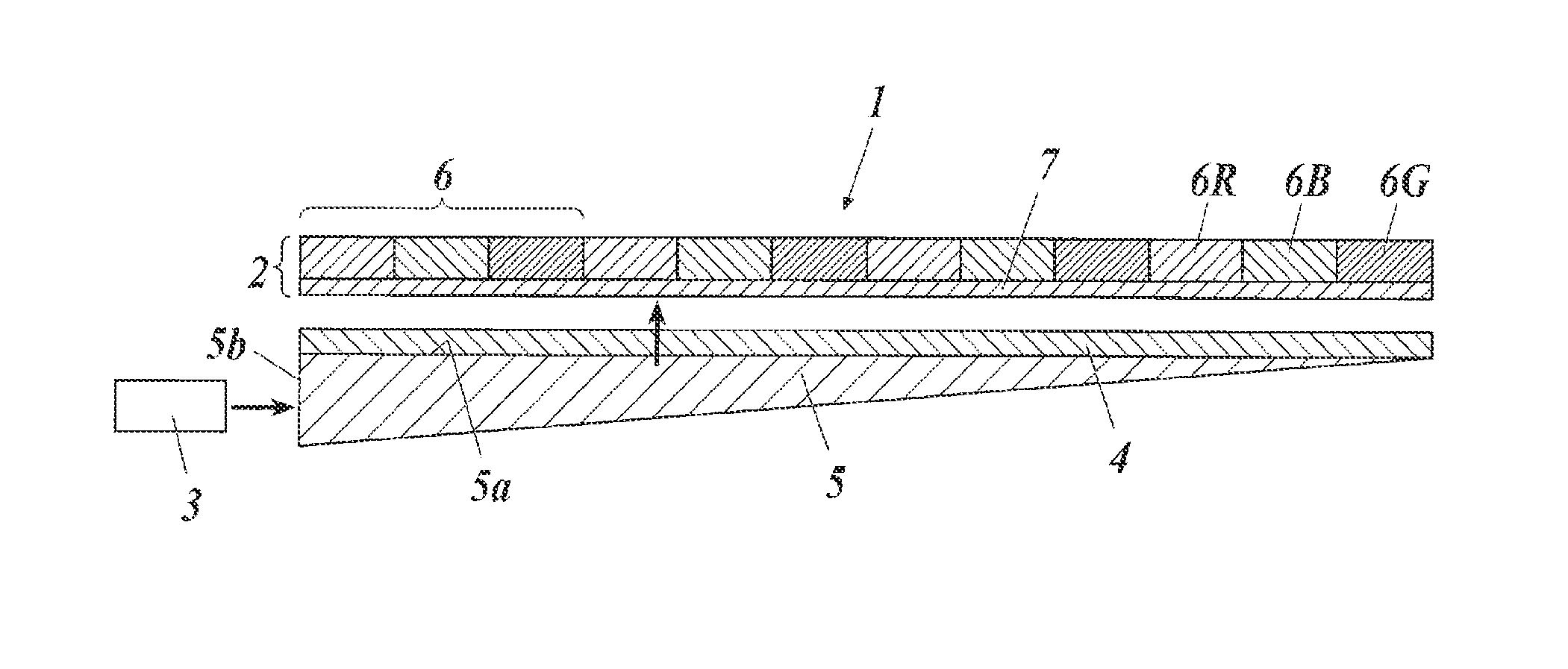
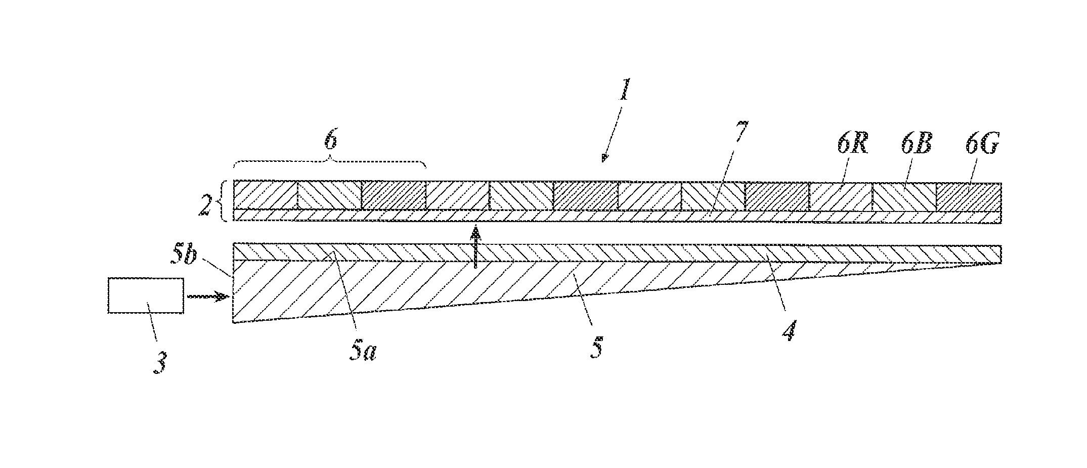
Image

Examples
example 1
Synthesis of Semiconductor Nanoparticles
Synthesis Example 1-1
Semiconductor Nanoparticles A1 (InP / ZnS)
[0177]Indium myristate (0.1 mmol), stearic acid (0.1 mmol), trimethylsilylphosphine (0.1 mmol), dodecanethiol (0.1 mmol), zinc undecylenate (0.1 mmol), and octadecene (8 mL) were placed in a three-neck flask, and the mixture was refluxed at 300° C. for one hour under a nitrogen atmosphere, to yield InP / ZnS (semiconductor nanoparticles A1). As used herein, semiconductor nanoparticles composed of an InP core and a ZnS shell are represented as “InP / ZnS.”
[0178]The semiconductor nanoparticles A1 were directly observed with a transmission electron microscope, and were determined to have an InP / ZnS core-shell structure such that the InP core was coated with the ZnS shell. This microscopic observation showed that the InP / ZnS semiconductor nanoparticles synthesized by the aforementioned process had a core particle size of 2.1 to 3.8 nm and a core particle size distribution of 6 to 40%. This o...
synthesis example 1-2
Silica-Coated Semiconductor Nanoparticles A2
[0180]The semiconductor nanoparticles A1 (0.4 mL, inorganic components: about 70 mg) were dried under vacuum.
[0181]Subsequently, triethyl orthosilicate (TEOS) (0.6 mL) was added to the semiconductor nanoparticles A1 to prepare a clear mixture, and the mixture was stored for incubation under N2 overnight. The mixture was then added to 10 mL of a reverse microemulsion (cyclohexane / CO-520 (surfactant described below), 18 mL / 1.35 g) in a 50-mL flask under agitation at 600 rpm. The mixture was agitated for 15 minutes, and then 4% NH4OH (0.1 mL) was added to the mixture for initiation of reaction. On the following day, the reaction was terminated through centrifugation, and the resultant solid phase was collected. The resultant particles were washed twice with cyclohexane (20 mL) and then dried under vacuum, to yield silica-coated semiconductor nanoparticles A2.
[0182]CO-520: Igepal (Registered Trademark) CO-520 (Nonionic Surfactant: Polyoxyethyl...
synthesis example 1-3
Silica-Coated Semiconductor Nanoparticles A3
[0184]The semiconductor nanoparticles A1 (0.4 mL, inorganic components: about 70 mg) were dried under vacuum. Subsequently, triethyl orthosilicate (TEOS) (0.6 mL) was mixed with aluminum triisopropoxide (0.3 mmol) under agitation at 80° C. for one hour. The mixture was added to the semiconductor nanoparticles A1 to prepare a clear mixture, and the mixture was stored for incubation under N2 overnight. The mixture was then added to 10 mL of a reverse microemulsion (cyclohexane / CO-520, 18 mL / 1.35 g) in a 50-mL flask under agitation at 600 rpm. The mixture was agitated for 15 minutes, and then 4% NH4OH (0.1 mL) was added to the mixture for initiation of reaction. On the following day, the reaction was terminated through centrifugation, and the resultant solid phase was collected. The resultant particles were washed twice with cyclohexane (20 mL) and then dried under vacuum, to yield silica-coated semiconductor nanoparticles A3.
[0185]The semico...
PUM
| Property | Measurement | Unit |
|---|---|---|
| particle size | aaaaa | aaaaa |
| particle size | aaaaa | aaaaa |
| transparency | aaaaa | aaaaa |
Abstract
Description
Claims
Application Information