
Phase synchronization of modulation or demodulation for QAM-based multiband TSV-link

Active Publication Date: 2016-05-26
RGT UNIV OF CALIFORNIA
View PDF12 Cites 1 Cited by
  • Summary
  • Abstract
  • Description
  • Claims
  • Application Information

AI Technical Summary

Benefits of technology

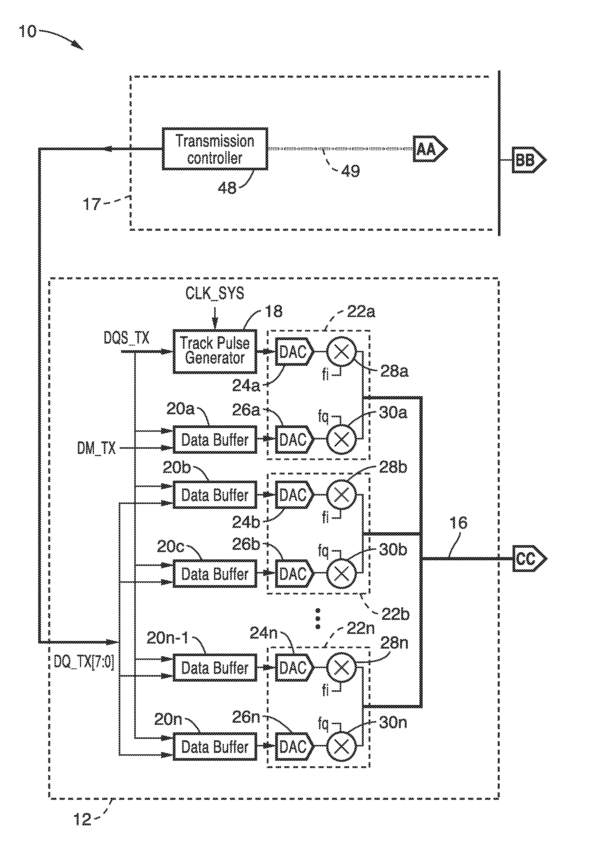
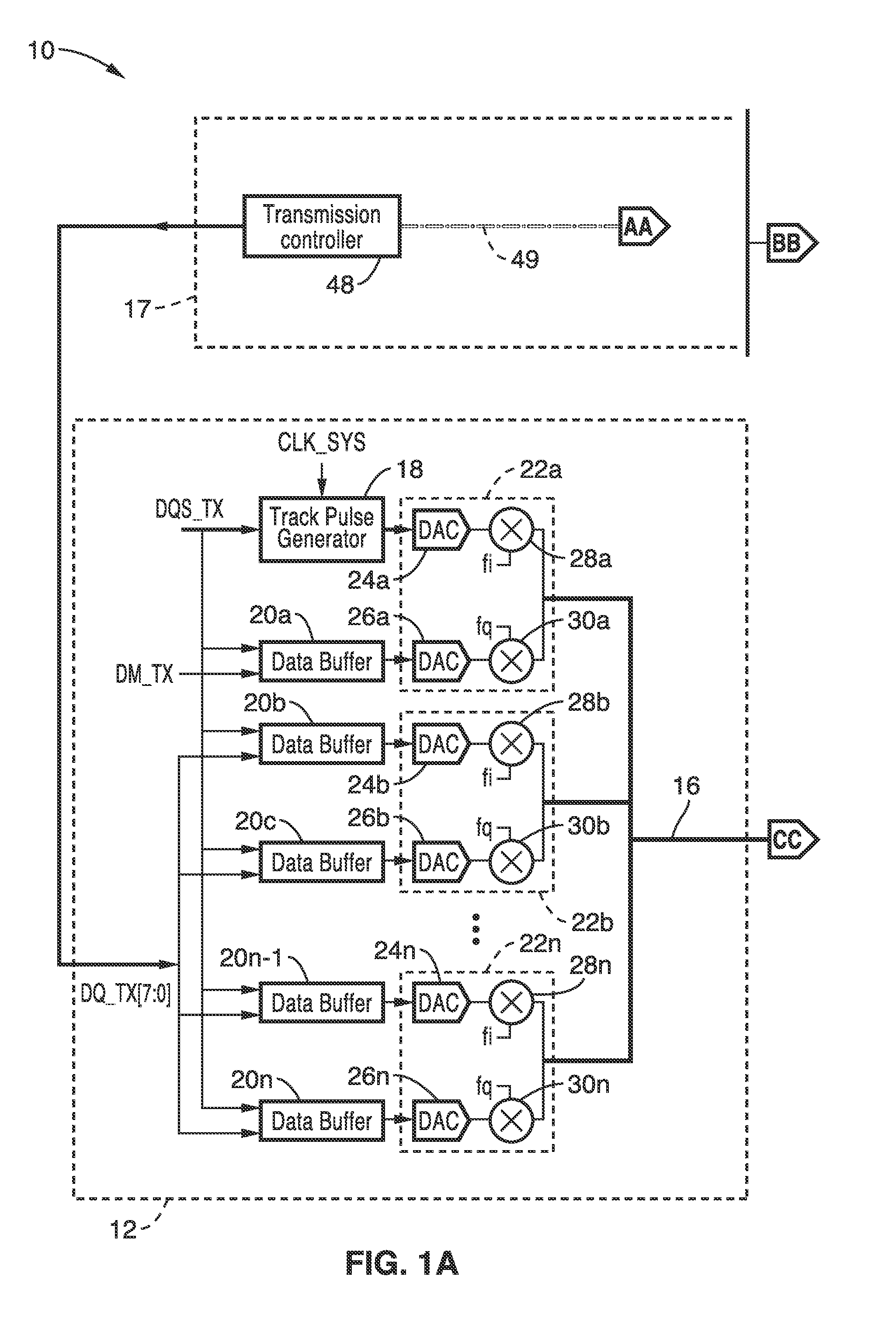
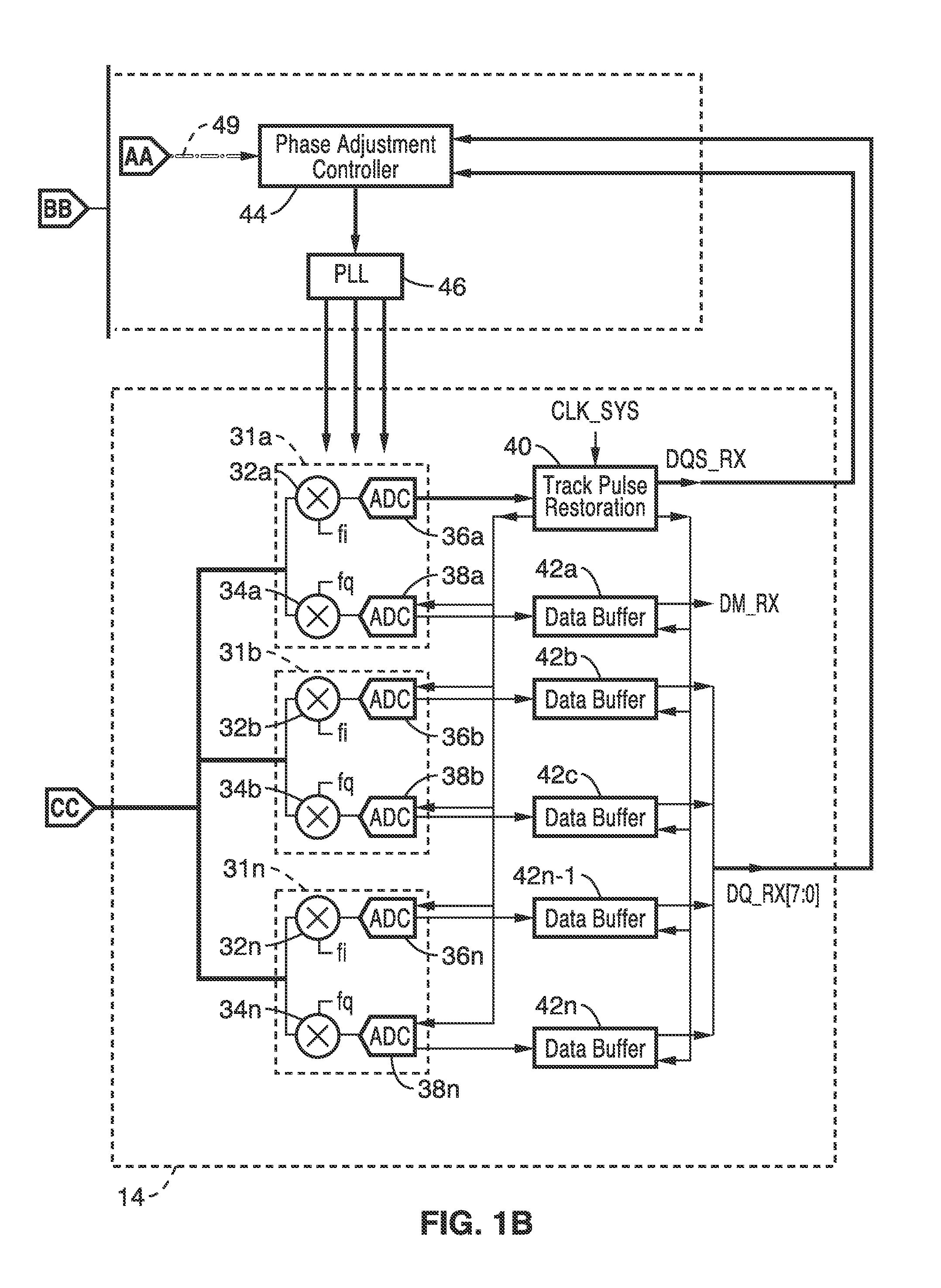
The patent is about a method to adjust the phase of a signal without using digital signal processing. This method is fast, requires simple equipment, and uses low power. It combines the action of a phase adjustment controller and a transmission controller to achieve the needed phase adjustment.

Problems solved by technology

However, each process technology has its own limitations on clock rates, whereby one must often increase the number of I / O connections to increase the bandwidth, and as a result manufacturing costs increase.
These costs are even further increased in 3D integrated circuit integration, such as those based on through-substrate-via (TSV) for vertical interconnections.
The number of TSVs for the I / O is non-scalable due to fundamental physical or mechanical constraints.
Higher than a certain number of TSVs per unit area (or population density) leads to thinned Si substrate (about 100 μm / tier) which can result in collapse.
Therefore, this thinning can seriously limit inter-tier communication bandwidth in 3D integrated circuits.
However, problems arise with these circuits when used in radio frequency (RF) communications in regard to phase synchronization for optimizing signal strength recovery.
Existing methods to perform this phase synchronization between modulation and demodulation is performed utilizing digital signal processing and requiring complex circuitry which is subject to high power consumption levels.
Although this traditional method offers flexibility of phase tuning capability by using software DSP, its long latency and large hardware overhead make the approach less preferable for short latency, low power, and simple circuit topologies, such as required for mobile and micro-server applications.

Method used


Image

  • Phase synchronization of modulation or demodulation for QAM-based multiband TSV-link
  • Phase synchronization of modulation or demodulation for QAM-based multiband TSV-link
  • Phase synchronization of modulation or demodulation for QAM-based multiband TSV-link

Examples


Embodiment Construction

[0019]Synchronization between modulation and demodulation is described for use in short-range chip-to-chip wired RF communication. The inventive apparatus, system and method provides a number of advantages, including lower power, lower latency, higher interference tolerance between neighboring through-Silicon-vias (TSVs).

[0020]Phase synchronization between modulation and demodulation carriers in RF communications is traditionally carried out through the use of digital signal processing. The demodulated signal is down converted to baseband and digitized by analog-to-digital converter. Then a digital signal processor (DSP) is utilized to perform the phase synchronization for the demodulated signal by using a digital-lock-loop (DLL) circuit. This conventional method requires a complicated algorithm implemented in DSP, which increases not only the latency of signal processing but also the power consumption.

[0021]In the presently described technology, a new method is described for perfor...


PUM


Abstract

A chip-to-chip communications circuit which is particularly well-suited for short range wired RF communication from one integrated circuit (chip) to another is presented. The circuits preferably utilize multi-frequency quadrature amplitude modulation (QAM) mechanisms for converting digital data bits from a parallel form into a serial analog stream for communication over a chip I / O connection. During a phase calibration cycle, a phase adjustment controller in the transmitter interoperates with a phase adjustment controller in the receiver, to adjust a phase locked-loop (PLL) circuit to correct for the phase delay arising in response to signal propagation between transmitter and receiver.

Description

CROSS-REFERENCE TO RELATED APPLICATIONS[0001]This application is a 35 U.S.C. §111(a) continuation of PCT international application number PCT / US2014 / 035818 filed on Apr. 29, 2014, incorporated herein by reference in its entirety, which claims priority to, and the benefit of, U.S. provisional patent application Ser. No. 61 / 827,094 filed on May 24, 2013, incorporated herein by reference in its entirety. Priority is claimed to each of the foregoing applications.[0002]The above-referenced PCT international application was published as PCT International Publication No. WO 2014 / 189651 on Nov. 27, 2014, which publication is incorporated herein by reference in its entirety.STATEMENT REGARDING FEDERALLY SPONSORED RESEARCH OR DEVELOPMENT[0003]Not ApplicableINCORPORATION-BY-REFERENCE OF COMPUTER PROGRAM APPENDIX[0004]Not ApplicableNOTICE OF MATERIAL SUBJECT TO COPYRIGHT PROTECTION[0005]A portion of the material in this patent document is subject to copyright protection under the copyright laws...

Claims


Application Information

Patent Timeline
IPC IPC(8): H04L27/34H04L27/36H04L7/033H04L27/38
CPCH04L27/3455H04L7/0331H04L27/364H04L27/3872H04L27/362H04L2027/0022H04L2027/0028H04L2027/0055H04L2027/0067
Inventor LEE, SHEAU JIUNGLI, YILEIHO, WEI-HANCHANG, MAU-CHUNG FRANK
Owner RGT UNIV OF CALIFORNIA
Learn More