Electrospun Nanofibrous Membranes and Disposable Glucose Biosensor
- Summary
- Abstract
- Description
- Claims
- Application Information
AI Technical Summary
Benefits of technology
Problems solved by technology
Method used
Image
Examples
embodiment 3
[0052]The producing method of a PVA / GOx / potassium hexacyanoferrate(III) / graphene oxide electrospun solution having steps of:
[0053]forming a 7 wt % PVA solution by mixing 7 g PVA and 93 g DI water; and
[0054]uniformly dispersing 14 mg GOx, 0.46 g of 0.25M potassium hexacyanoferrate(III) solution and 0.5% graphene oxide solution into 10 g of 7 wt % PVA solution to form the PVA / GOx / potassium hexacyanoferrate(III) / nano-gold electrospun solution.
[0055]The parameters of electrospinning are varied to reach suitable properties of electrospun nanofibrous membranes. The preferred embodiment of electrospinning parameters in the present invention may be applying 10 kV˜40 kV voltage, 0.1˜0.6 (ml / hr) flow rate, 10 cm˜25 cm distance from a catching screen to a extruded opening, 1˜2 hrs electrospining time or 40+ / −5% relative humidity. The electrospun nanofibrous membrane is spun on a PET film.
[0056]Preferred embodiments of disposable glucose biosensor in present invention are as followings.
embodiment 1
[0057]The producing method of the disposable glucose biosensor in present invention comprising steps of:
[0058]detaching the nanofibrous membrane of the PET film; and
[0059]attaching the nanofibrous membrane on the screen-printed carbon electrode to form the disposable glucose biosensor.
embodiment 2
[0060]The producing method of a cross-linked disposable glucose biosensor in present invention comprising steps of:
[0061]cross-linking the nanofibrous membrane by the ultra sound assistance cross-linked method with glutaraldehyde vapor;
[0062]detaching the cross-linked nanofibrous membrane of the PET film; and
[0063]attaching the cross-linked nanofibrous membrane on the screen-printed carbon electrode to form the disposable glucose biosensor.
[0064]Physical appearance, chemical properties and electrochemical properties of the present invention and the comparison with the conventional non-electrospun PVA film are as followings. The testing devices are an electrochemical analyzer, a scanning electron microscope (SEM) and a transmission electron microscopy (TEM).
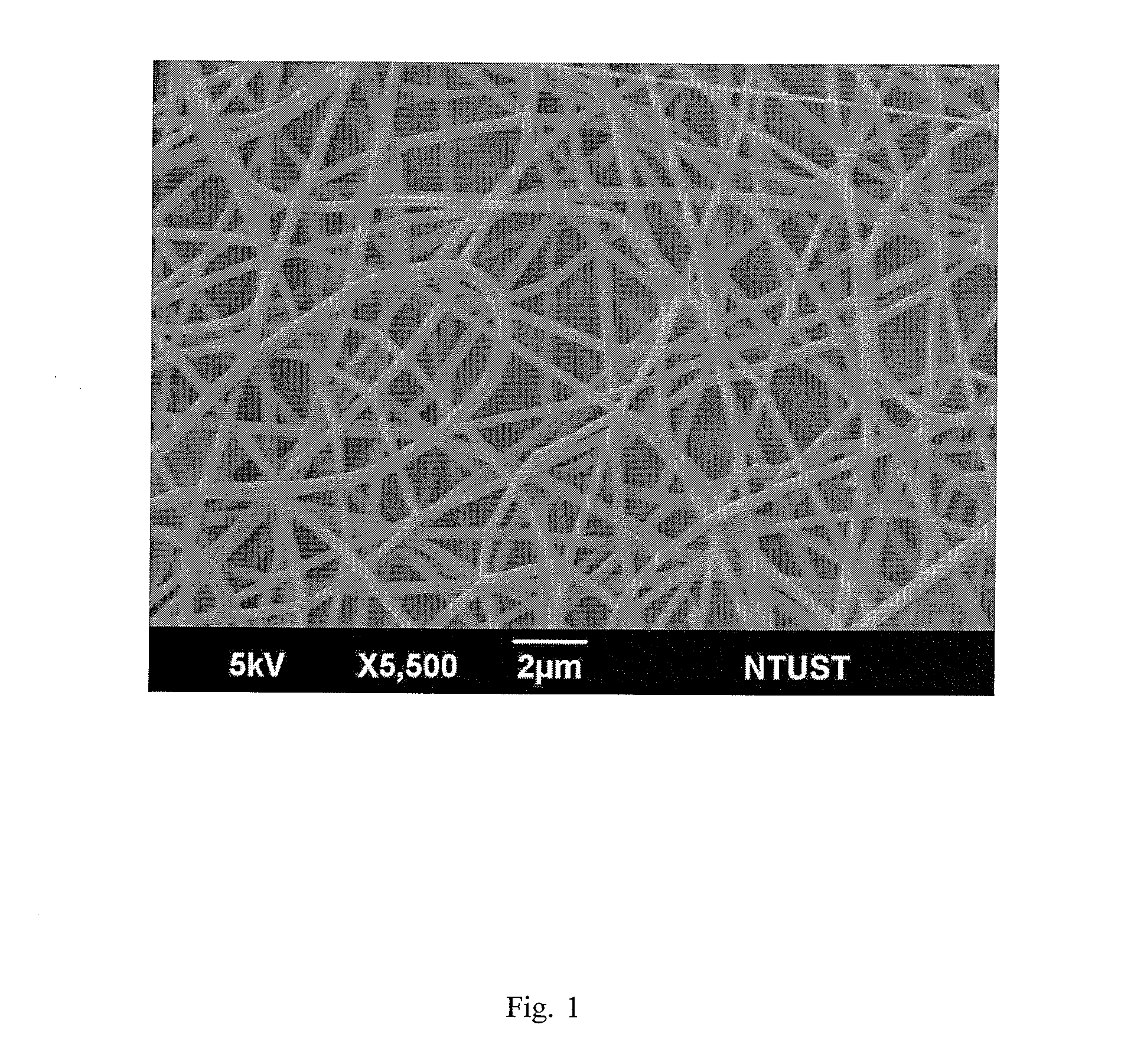
[0065]With reference to FIG. 1, SEM pattern shows average diameter of the present invention is about 296+ / −48 nm. With reference to FIG. 14, SEM pattern shows surface appearance of the conventional non-electrospun PVA film. Surfac...
PUM
| Property | Measurement | Unit |
|---|---|---|
| Fraction | aaaaa | aaaaa |
| Fraction | aaaaa | aaaaa |
| Fraction | aaaaa | aaaaa |
Abstract
Description
Claims
Application Information


