Ferroelectric memory device and fabrication process thereof, and methods for operation thereof

a ferroelectric memory and fabrication process technology, applied in the field of memory devices and photonics, can solve the problems of ferroelectric materials, lithium niobate, and difficult to manufacture on the nano-scale properly, and achieve the effects of improving the efficiency of production and maintenance, reducing the cost of production, and improving the quality of production

Inactive Publication Date: 2016-06-16
MCKINNON THOMAS J +1
View PDF0 Cites 24 Cited by
  • Summary
  • Abstract
  • Description
  • Claims
  • Application Information

AI Technical Summary

Benefits of technology

[0019]When the ferroelectric layer is thin enough, from one monolayer (approximately ˜0.2 nm) to approximately 5 nm, another phenomenon acts to further change the resistance of the memory cell when ferroelectric polarization is reversed. When the ferroelectric layer is this thin, electrons have a significant probability to tunnel through the ferroelectric layer. In this case the ferroelectric layer would cause a potential barrier for the electrons. The probability of the electrons to tunnel through the p...

Problems solved by technology

That is, server farms require low cost high-density memory, mobile devices require low power memory, and supercomputers require high speed memory.
However, many ferroelectric materials, i...

Method used


Image

  • Ferroelectric memory device and fabrication process thereof, and methods for operation thereof
  • Ferroelectric memory device and fabrication process thereof, and methods for operation thereof
  • Ferroelectric memory device and fabrication process thereof, and methods for operation thereof

Examples


first embodiment

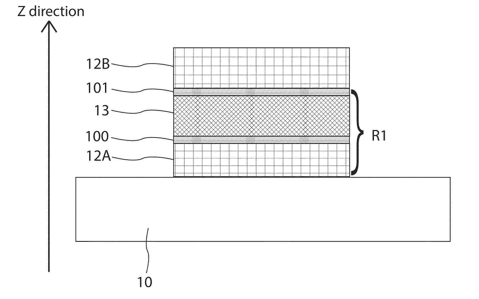
[0055]FIG. 1 shows the construction of a ferroelectric memory device according to the first embodiment of the present invention.

[0056]Going from bottom to top, the first embodiment consists of a substrate 10, a bottom electrode 12A, a Schottky modulating interlayer 100, a ferroelectric layer 13, a Schottky modulating interlayer 101, and a top electrode 12B. The present embodiment also contains a section of layers labeled R1, which can be repeated n times where n is any number from 0 to infinity.

[0057]The substrate layer 10 acts as a platform to grow the rest of the structure on top of. The substrate layer generally consist of undoped silicon, or N or P doped silicon. The substrate layer can also consist of an electronic layer containing transistors with a bit and word line to select single memory cells. In this case, the memory cell will sit above the transistors in such a way as to allow current and voltage to be sent to a single memory cell without disturbing the others. The subst...

second embodiment

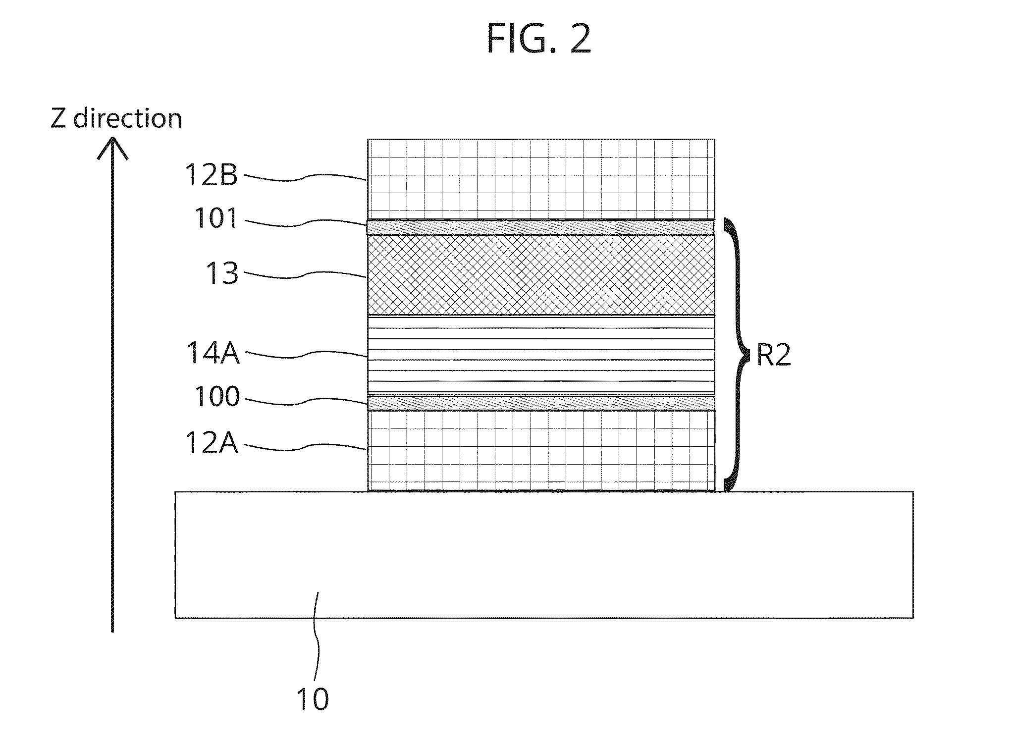
[0120]FIG. 2 shows the construction of a ferroelectric memory device according to the second embodiment of the present invention.

[0121]Going from bottom to top, the second embodiment consists of a substrate 10, a bottom electrode 12A, a Schottky modulating interlayer 100, a semiconductor layer 14A, a ferroelectric layer 13, a Schottky modulating interlayer 101, and a top electrode 12B. The present embodiment also contains a section of layers labeled R2, which can be repeated n times where n is any number from 0 to infinity.

[0122]All of the layers, except for the semiconductor layer 14A, are exactly as described for the first embodiment. The names of the other layers have remained the same as in the first embodiment to show that they are identical. Additionally, the repeating layer is now labeled R2, but can be repeated in the same manner as described in the first embodiment.

[0123]The layer 14A can consists of at least one of the following semiconductor materials: silicon (Si), germa...

third embodiment

[0125]FIG. 3 shows the construction of a ferroelectric memory device according to the third embodiment of the present invention.

[0126]Going from bottom to top, the third embodiment, consists of a substrate 10, a bottom electrode 12A, a Schottky modulating interlayer 100, a ferroelectric layer 13, a semiconductor layer 14B, a Schottky modulating interlayer 101, and a top electrode 12B. The present embodiment also contains a section of layers labeled R3, which can be repeated n times where n is any number from 0 to infinity.

[0127]All of the layers are exactly as described for the second embodiment except the layer 14A has been moved to the top of the ferroelectric layer and is now called 14B. It is still described in exactly the same way as 14A was in the second embodiment. The names of the other layers have remained the same as in the first embodiment to show that they are identical. Additionally, the repeating layer is now labeled R3, but can be repeated in the same manner as descri...


PUM


Abstract

A new form of a solid-state non-volatile memory cell is presented. The solid-state memory cell comprises a series of different layers of ferroelectric materials, semiconductors, ferroelectric semiconductors, metals, and ceramics, and oxides. The memory device stores information in the direction and magnitude of polarization of the ferroelectric layers. Additionally, a method is presented for storing multiple bits of information in a single memory cell by allowing partial polarization of a single ferroelectric layer and stacking of multiple ferroelectric functional units on top of each other. Additionally, a technique for reading and writing said memory cell is presented. Additionally, the memory cell design allows for the formation of Schottky barriers which act to improve functionality and increase resistance. Additionally, a method is presented for depositing textured lithium niobate thin films.

Description

CROSS-REFERENCE TO RELATED APPLICATIONS[0001]This is a non-provisional utility application claiming benefit of previously filed provisional application with application No.: 62 / 074,047 on date: 2014 Nov. 2, titled: Ferroelectric memory device.BACKGROUND OF THE INVENTION[0002]The present invention generally pertains to two fields of endeavor: memory devices and photonics. More particularly, the present invention pertains to ferroelectric memory cells that store information in the direction of polarization of a ferroelectric film, and secondly, electronic or photonic devices that source, detect, modify, and control light.[0003]The civilized world has a great need to store information for one purpose or another, and all of the information is stored in memory devices of one form or another. Supercomputers, cloud storage infrastructure, personal computers, mobile phones and more all require memory to function. Each application generally requires memory that is specifically designed for i...

Claims


Application Information

Patent Timeline
IPC IPC(8): H01L27/115G11C11/22
CPCH01L27/11507G11C11/2273G11C11/2275G11C11/223H01L28/40H10B53/30
Inventor MCKINNON, THOMAS J.GIRT, EROL
Owner MCKINNON THOMAS J
Why Eureka
Try Eureka