Cleaning composition and method for cleaning semiconductor wafers after cmp

Active Publication Date: 2016-07-14
CMC MATERIALS INC
View PDF0 Cites 11 Cited by
  • Summary
  • Abstract
  • Description
  • Claims
  • Application Information

AI Technical Summary

Benefits of technology

The invention provides a composition for removing contaminants from semiconductor wafers after chemical-mechanical polishing. The composition contains quaternary ammonium hydroxides to regulate pH, organic amines, metal inhibitors, and water. The cleaning method involves contacting the surface of the semiconductor wafer with the composition to remove the contaminants. The invention also provides a method for polishing and cleaning the surface of a semiconductor wafer by using a polishing pad and a chemical-mechanical polishing composition to abrade the surface of the semiconductor wafer and remove contaminants, followed by contacting the polished surface with a cleaning composition to remove any remaining contaminants.

Problems solved by technology

Although conventional CMP processes are suitable for polishing, they tend to leave undesirable contaminants on the wafer surface.
In particular, the wafer surface is often contaminated with remnants of the polishing composition, such as silica or alumina abrasive particles, and with metal ions from the polishing composition and from the material being polished.
Such contaminants can have an adverse effect on semiconductor wafer performance.
Typical post-CMP cleaning compositions have not been fully satisfactory in cleaning semiconductor wafers.
For example, it has been a challenge to obtain a cleaning solution that effects both low corrosion and good cleaning of material being polished.

Method used


Image

  • Cleaning composition and method for cleaning semiconductor wafers after cmp
  • Cleaning composition and method for cleaning semiconductor wafers after cmp
  • Cleaning composition and method for cleaning semiconductor wafers after cmp

Examples


example 2

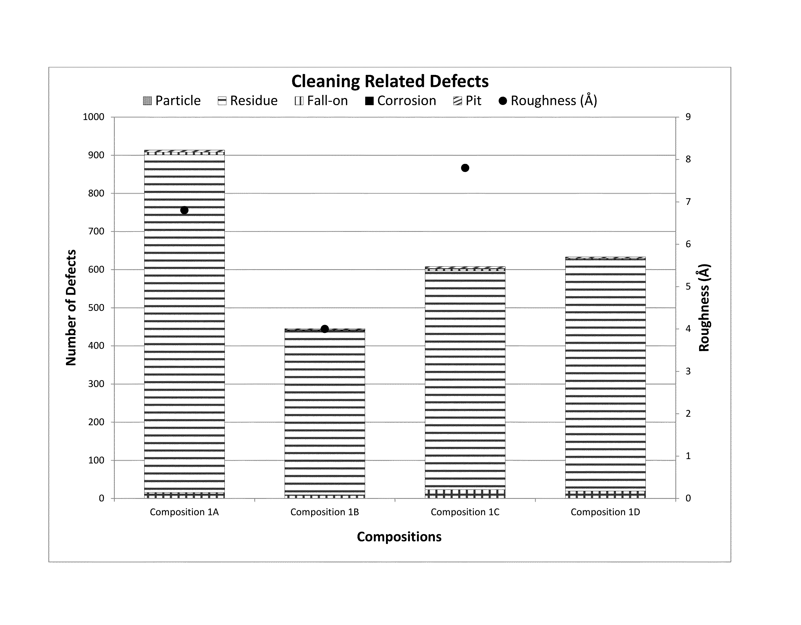
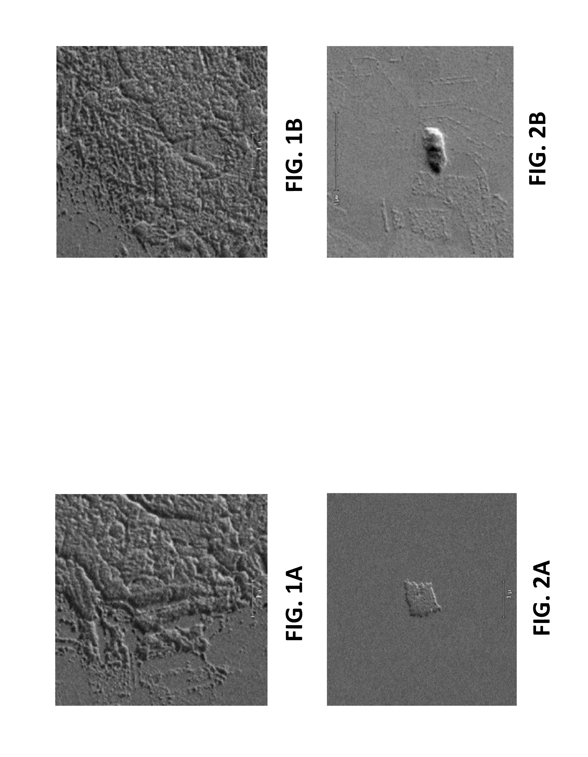
[0118]This Example compares the effectiveness of a cleaning composition compared in accordance with embodiments of the invention with different cleaning compositions after chemical-mechanical polishing (“CMP”) has taken place on a wafer substrate containing copper.

[0119]In particular, blanket wafers (i.e., without any patterns) containing copper were subjected to P2 copper polishing and P3 barrier polishing as described in Example 1.

[0120]As recited below in Table 3, three cleaning compositions, designated 2A-2C, were prepared with either tetraethylammonium hydroxide (TMAH) or tris(2-hydroxyethyl)methylammonium hydroxide (THEMAH) as a base, either monoethanolamine (MEA) or Ethylenediamine (En) as an organic amine, and diethylhydroxylamine (DEHA) as an antioxidant. Composition 2A, commercially available as Clean8158T™, was prepared, for purposes of comparison, with an etchant containing triphosphonic acid commercially available as Dequest 2000™ (D2000) from Dequest Italmatch Chemical...

example 3

[0125]This Example compares the effectiveness of a cleaning composition compared in accordance with embodiments of the invention with different cleaning compositions after chemical-mechanical polishing (“CMP”) has taken place on a wafer substrate containing copper.

[0126]In particular, blanket wafers (i.e., without any patterns) containing copper were subjected to P2 copper polishing and P3 barrier polishing as described in Example 1.

[0127]As recited below in Table 5, two cleaning compositions, designated 3A-3B, were prepared with either tetraethylammonium hydroxide (TMAH) or tris(2-hydroxyethyl)methylammonium hydroxide (THEMAH) as a base, either monoethanolamine (MEA) or 1,2-diaminopropane (Pn) as an organic amine, and diethylhydroxylamine (DEHA) as an antioxidant. Composition 3A, commercially available as Clean8158T™, was prepared, for purposes of comparison, with an etchant containing triphosphonic acid commercially available as Dequest 2000™ (D2000) from Dequest Italmatch Chemica...

example 4

[0132]This Example compares the effectiveness of a cleaning composition compared in accordance with embodiments of the invention with different cleaning compositions after chemical-mechanical polishing (“CMP”) has taken place on a wafer substrate containing copper.

[0133]In particular, blanket wafers (i.e., without any patterns) containing copper were subjected to P2 copper polishing and P3 barrier polishing as described in Example 1.

[0134]As recited below in Table 7, three cleaning compositions, designated 4A-4B, were prepared with either tetraethylammonium hydroxide (TMAH) or tris(2-hydroxyethyl)methylammonium hydroxide (THEMAH) as a base, either monoethanolamine (MEA) or 1,2-diaminopropane (Pn) as an organic amine, and diethylhydroxylamine (DEHA) as an antioxidant. Composition 4A, commercially available as Clean8158T from CMC, was prepared, for purposes of comparison, with an etchant containing triphosphonic acid commercially available as Dequest 2000™ (D2000) from Dequest Italmat...


PUM


Abstract

The invention provides a composition for cleaning contaminants from semiconductor wafers following chemical-mechanical polishing. The cleaning composition contains one or more quaternary ammonium hydroxides, one or more organic amines, one or more metal inhibitors, and water. The invention also provides methods for using the cleaning composition.

Description

BACKGROUND OF THE INVENTION[0001]A semiconductor wafer is typically composed of a substrate, such as a silicon wafer, on which a plurality of transistors have been formed. Transistors are chemically and physically connected into a substrate and are interconnected through the use of well-known multilevel coplanar interconnects to form functional circuits. Typical multilevel interconnects are comprised of stacked thin-films consisting of, for example, one or more of the following: titanium (Ti), titanium nitrate (TiN), copper (Cu), aluminum (Al), tungsten (W), tantalum (Ta), cobalt (Co), ruthenium (Ru), or any combination thereof.[0002]The traditional technique for forming functional multilevel coplanar interconnects has involved planarizing the surface of the interconnects via chemical-mechanical polishing (CMP). CMP involves the concurrent chemical and mechanical polishing of an overlying first layer to expose the surface of a non-planar second layer on which the first layer has bee...

Claims


Application Information

Patent Timeline
IPC IPC(8): C11D11/00H01L21/02C11D7/32
CPCC11D11/0047C11D7/3218H01L21/02074C11D7/3272C11D7/3281C11D7/3209C11D7/06C11D2111/22C11D3/0073C11D7/261C11D7/265C11D7/32C11D7/329C11D7/34H01L21/02052
Inventor IVANOV, ROMANHUNG, FERNANDOKO, CHENG-YUANSUN, FRED
Owner CMC MATERIALS INC
Why Eureka
Try Eureka