3D integrated circuit

a technology of integrated circuits and integrated circuits, applied in the field of three-dimensional (3d) integrated circuits, can solve the problems of dramatic degradation of overall system performance, congestion of routing, and difficulty in dissipating heat, so as to improve overall system performance, reduce total power consumption, and low cost

Active Publication Date: 2016-07-21
QUALCOMM INC
View PDF4 Cites 12 Cited by
  • Summary
  • Abstract
  • Description
  • Claims
  • Application Information

AI Technical Summary

Benefits of technology

[0009]In accordance with the teachings herein, 3D-ICs with TSVs may be used to address advanced semiconductor device scaling problems. Through the use of 3D-ICs, multiple dies with the same and/or different technologies can be integrated i

Problems solved by technology

Existing 3D-IC routing design faces several critical challenges relating to power distribution network (PDN) design, thermal management, and testing methodology.
This PDN occupies significant die area and leads to routing congestion.
Regarding thermal management, when multiple dies are stacked together, it is difficult to dissipate

Method used


Image

  • 3D integrated circuit
  • 3D integrated circuit
  • 3D integrated circuit

Examples


example electronic

Device

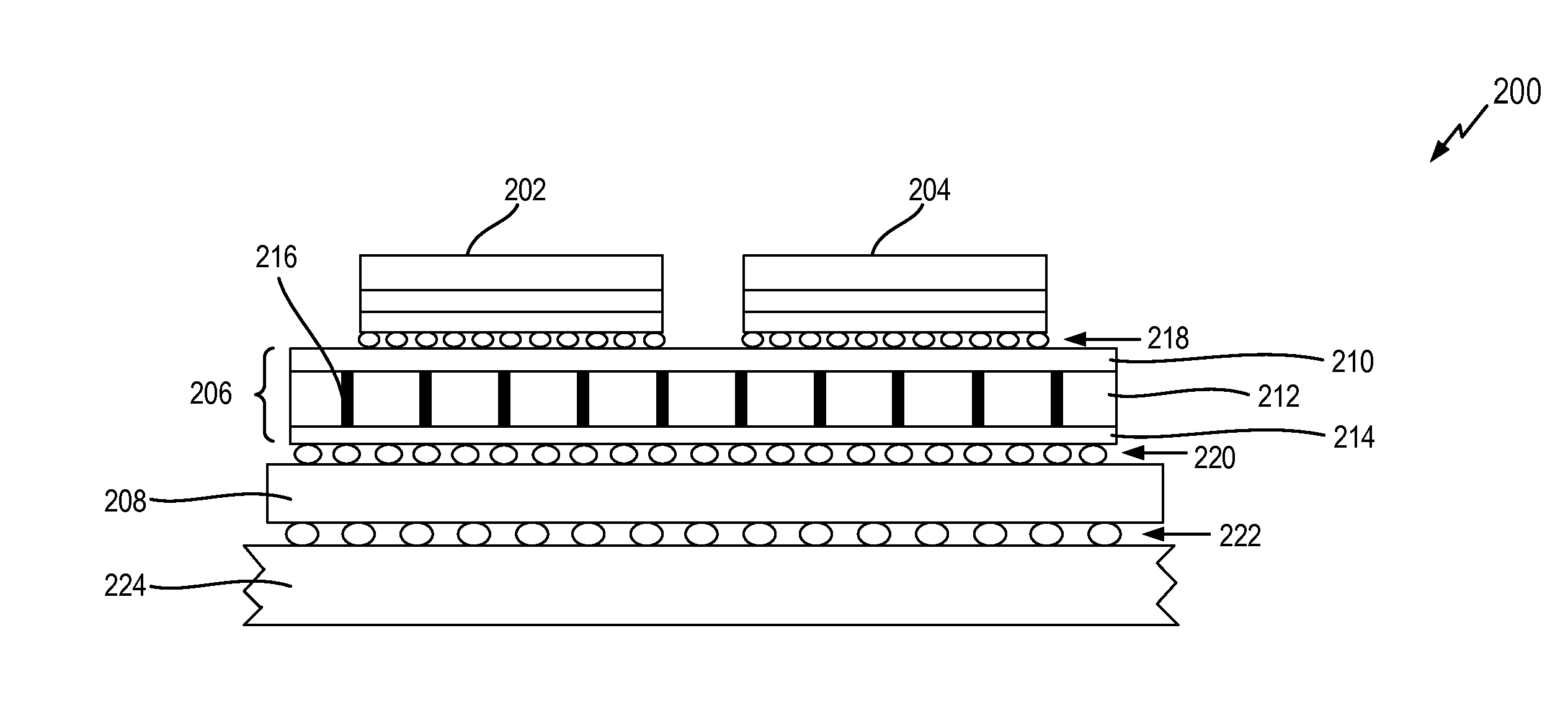
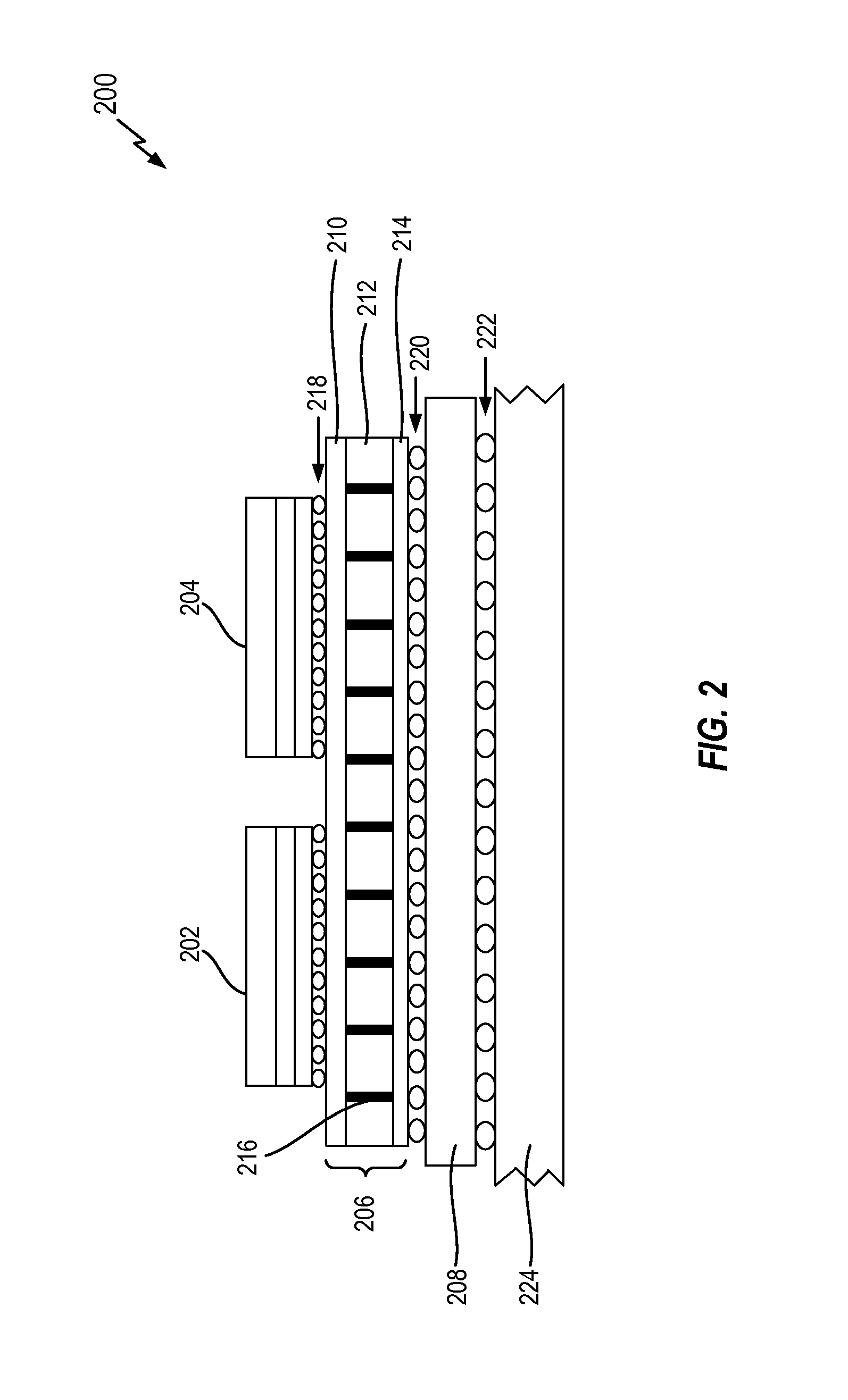
[0108]FIG. 21 is an illustration of an apparatus 2100 that may be implemented as a 3D-IC according to one or more aspects of the disclosure. The apparatus 2100 includes a communication interface (e.g., at least one transceiver) 2102, a storage medium 2104, a user interface 2106, a memory device 2108, and a processing circuit 2110.

[0109]These components can be coupled to and / or placed in electrical communication with one another via a signaling bus or other suitable component, represented generally by the connection lines in FIG. 21. The signaling bus may include any number of interconnecting buses and bridges depending on the specific application of the processing circuit 2110 and the overall design constraints. The signaling bus links together various circuits such that each of the communication interface 2102, the storage medium 2104, the user interface 2106, and the memory device 2108 are coupled to and / or in electrical communication with the processing circuit 2110. The si...

example processes

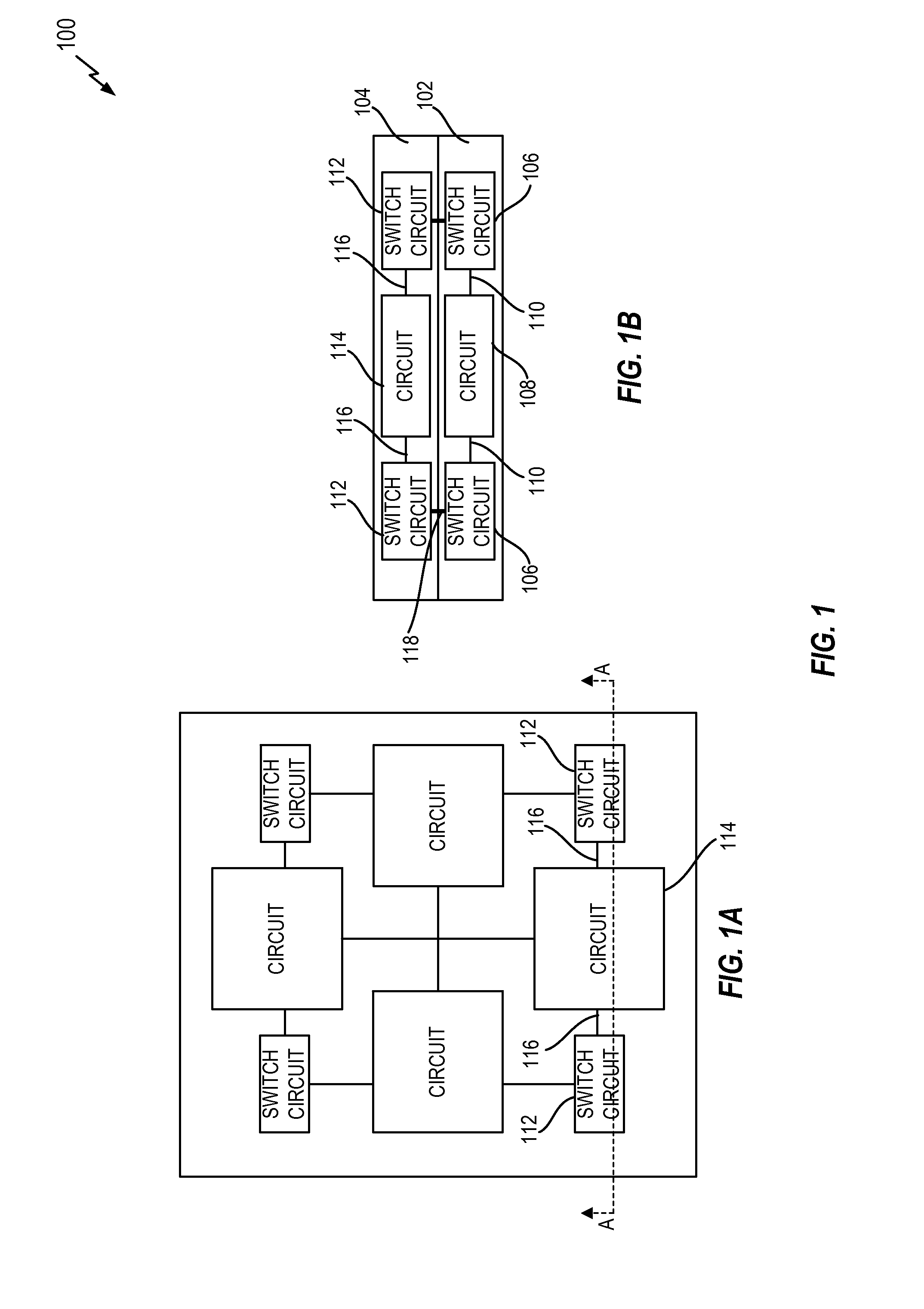
[0124]FIG. 22 illustrates a switching process 2200 in accordance with some aspects of the disclosure. The process 2200 may take place within a 3D-IC (e.g., one or more of the 3D-IC of any of FIG. 1, 5, 6, or 9-21), at least partially within a processing circuit (e.g., the processing circuit 2110 of FIG. 21), which may be located in an electronic device, a transceiver, or some other suitable apparatus. Of course, in various aspects within the scope of the disclosure, the process 2200 may be implemented by any suitable apparatus capable of supporting switching operations.

[0125]At block 2202, a signal is received via a first signal path at a first switch circuit. The first switch circuit is on a first die that lies within a first geometric plane.

[0126]The signal may take different forms in different implementations. In some aspects, the signal may be a test signal (e.g., that is selectively routed between first and second dies). In some aspects, the signal may be a power supply voltage...


PUM


Abstract

A three-dimensional integrated circuit (3D-IC) architecture incorporates multiple layers, each layer including at least one die and at least one switch to connect the dies on the different layers. In some aspects, a power distribution network (PDN) is routed from a first layer through the switches to supply power to at least one other layer, thereby reducing routing congestion on the layers. The switches can be placed around the periphery of an IC package to improve heat dissipation (e.g., by improving heat transfer from the center to the edge of the IC package). The switches can be used for routing test signals and/or other signals between layers, thereby improving test functionality and/or fault recovery.

Description

BACKGROUND[0001]1. Field of the Disclosure[0002]Aspects of the disclosure relate generally to electronic circuits, and more specifically, but not exclusively, to a three-dimensional (3D) integrated circuit (IC).[0003]2. Description of Related Art[0004]Conventional 3D integrated circuit (3D-IC) architectures include a so-called 2.5D architecture and a fully stacked 3D architecture. In a 2.5D architecture, dies are placed side-by-side and interconnected via a horizontal interposer layer. A fully stacked 3D architecture employs dies that are stacked on top of one another. Both architectures use through-silicon vias (TSVs) to connect the metal layers.[0005]Existing 3D-IC routing design faces several critical challenges relating to power distribution network (PDN) design, thermal management, and testing methodology. A typical 3D-IC PDN is implemented as a pyramid shape where power rails are used to supply the power from the bottom of the IC to the top of the IC. This PDN occupies signifi...

Claims


Application Information

Patent Timeline
IPC IPC(8): H01L25/065H03K17/56H03K17/00
CPCH01L25/0657H03K17/56H03K17/002G11C29/1201G11C29/48H01L2225/06572H01L2225/06541H01L2225/06596H01L2924/0002H01L2225/06513H01L2924/00H01L23/5384H01L23/5385H01L22/32G01R31/318513H01L2224/13025H01L2224/16146H01L2224/16227H01L2224/17181
Inventor LAW, OSCARLIU, CHUNCHENLU, JU-YI
Owner QUALCOMM INC
Why Eureka
Try Eureka