

Methods for producing a thin film ferroelectric device using a two-step temperature process
a thin film, temperature process technology, applied in the direction of thermoelectric devices, solid-state devices, coatings, etc., can solve the problems of affecting the stable operation of the film, the current available processes continue to arise, and the nano-size cracks routinely developing on the pvdf film, etc., to reduce the interfacial void or crack in the resulting material, reduce the interfacial void, and improve the durability of the ferroelectric film used
- Summary
- Abstract
- Description
- Claims
- Application Information
AI Technical Summary
Benefits of technology
Problems solved by technology
Method used
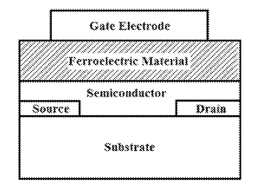
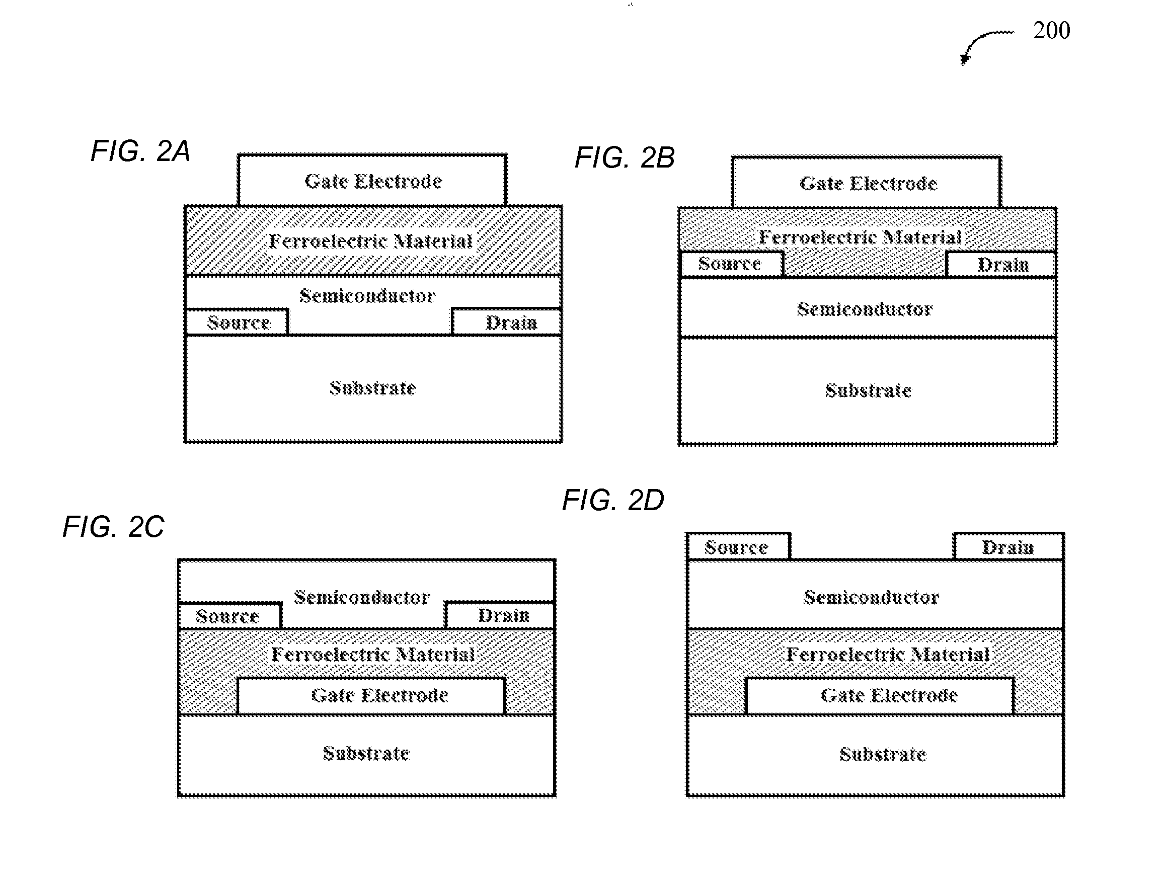
Image

Examples
example 1
Fabrication of Ferroelectric Device with 2-Step Temperature Process
[0096]A ferroelectric capacitor of the present invention was fabricated using a two-step temperature process using the following method.
[0097]Polymer Solution.
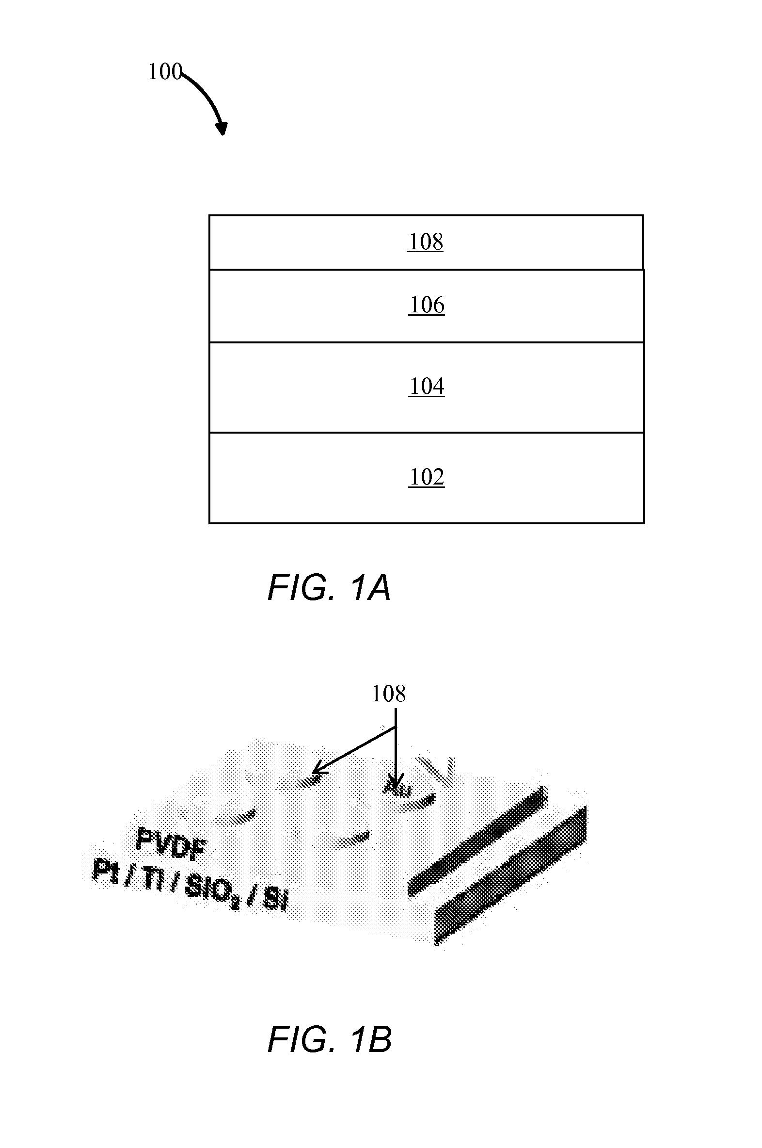
[0098]A solution of PVDF in solvent was prepared by adding PVDF powder (Sigma Aldrich®, MW=534,000 g / mol) to dimethylformamide solvent (Sigma Aldrich®). The solution was filtered using a polytetrafluoroethylene filter (1 μm pore size). The PVDF solution was stirred and heated at 110° C. using a conventional hot-plate for about 20 min to completely dissolve the PVDF. This heating of the PVDF solution ensured that the spin-coated PVDF thin-films would be uniform.
[0099]Ferroelectric Capacitor.
[0100]A bottom electrode (25 nm-thick Pt (25 nm) / Ti (5 nm)) was sputter deposited on SiO2 (100 nm silicon). The bottom electrode and substrate was added to a spin coating apparatus. The hot polymer solution was deposited on the bottom electrode at a rate of 4000 rpm for 60 se...
example 2
Testing of Ferroelectric Devices of Example 1
[0101]Ferroelectric Hysteresis Properties During Annealing Process.
[0102]Hysteresis loops for the ferroelectric devices of the present invention made in Example 1, were measured before and after the 2-step temperature process at a frequency of 100 Hz and are depicted in FIGS. 12A and 12B. FIG. 12A is a graphical depiction of the polarization (μC / cm2) versus electric field (MV / m) at 100 Hz for a ferroelectric device of the present invention before starting the 2-step temperature process. FIG. 12B is a graphical depiction of the polarization (μC / cm2) versus electric field (MV / m) at 100 Hz for a ferroelectric capacitor of the present invention after the two step temperature process. Comparing FIG. 12A to FIG. 12B, the hysteresis loop in FIG. 12B was more defined than for the hysteresis for the ferroelectric material in FIG. 12A, and thus demonstrating an improvement of the hysteresis properties of the ferroelectric material due to the two-st...
PUM
| Property | Measurement | Unit |
|---|---|---|
| temperature | aaaaa | aaaaa |
| temperature | aaaaa | aaaaa |
| temperature | aaaaa | aaaaa |
Abstract
Description
Claims
Application Information