Substrate having annealed aluminum nitride layer formed thereon and method for manufacturing the same

a technology of aluminum nitride and substrate, which is applied in the direction of lasers, semiconductor devices, semiconductor lasers, etc., can solve the problems of large number of threading dislocations in the aln layer grown on sapphire, and achieve the effects of high efficiency, and improving the crystalline properties of the aln layer

Active Publication Date: 2016-09-01
TOHOKU UNIV +1
View PDF1 Cites 29 Cited by
  • Summary
  • Abstract
  • Description
  • Claims
  • Application Information

AI Technical Summary

Benefits of technology

[0012]The present invention takes into account these problems, and an object thereof is to provide a substrate having an aluminum nitride (AlN) layer and a method for manufacturing an aluminum nitride (AlN) layer by which it is possible to drastically improve crystalline properties of an AlN layer using growth conditions of the currently used MOCVD method without the need for complex processes such as forming grooves in a sapphire substrate, thereby being able to form a high efficiency light-emitting diode (LE...

Problems solved by technology

AlN has a large lattice mismatch with sapphire, and thus, an AlN...

Method used


Image

  • Substrate having annealed aluminum nitride layer formed thereon and method for manufacturing the same
  • Substrate having annealed aluminum nitride layer formed thereon and method for manufacturing the same
  • Substrate having annealed aluminum nitride layer formed thereon and method for manufacturing the same

Examples


example 1

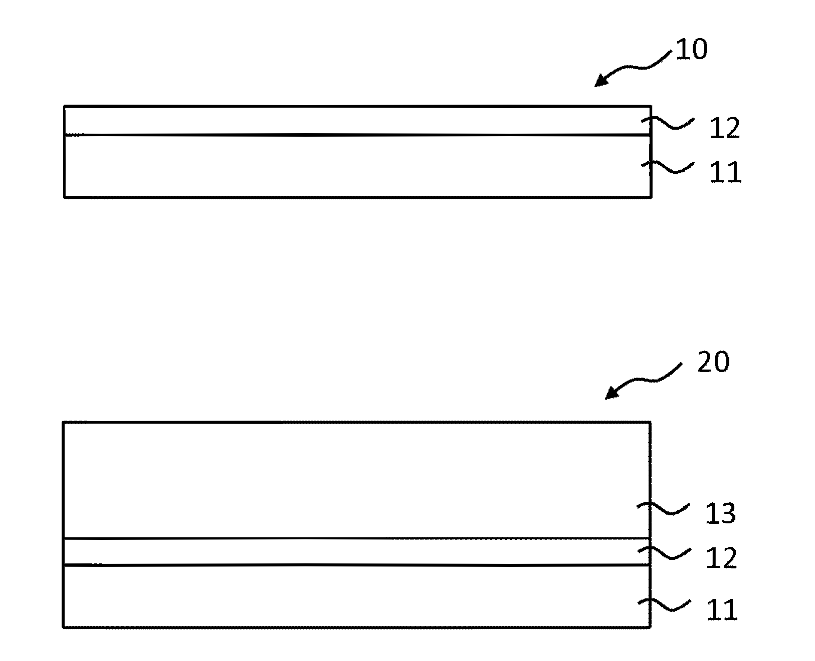
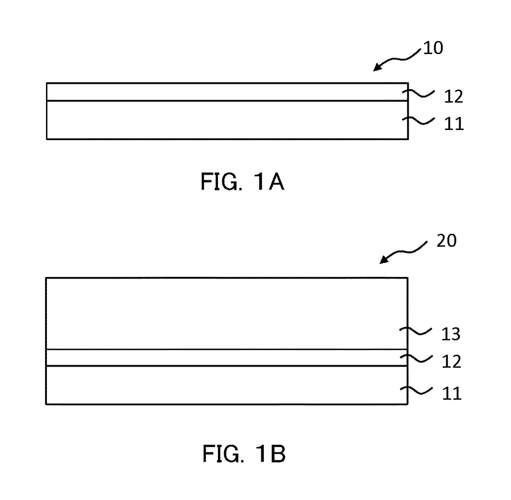
[0080]First, an AlN layer was formed to approximately 300 nm by MOVPE on the c surface of the sapphire substrate having a diameter of 2 inches, at a growth temperature of 1150° C. The crystalline properties of the AlN layer were as follows: the FWHM of the XRC of the (0002) AlN was 90 arcsec, the FWHM of the XRC of the (10-12) AlN was 1278 arcsec, and the FWHM of the XRC of the (10-10) AlN was 1508 arcsec. Also, the roughness mean square (RMS) of the surface was 3.10 nm. This AlN / sapphire substrate was divided into four equal parts, of which one piece was annealed as follows. (0002), (10-12), and (10-10) show an AlN crystalline lattice surface having a wurtzite structure according to four axes using a Miller coefficient.

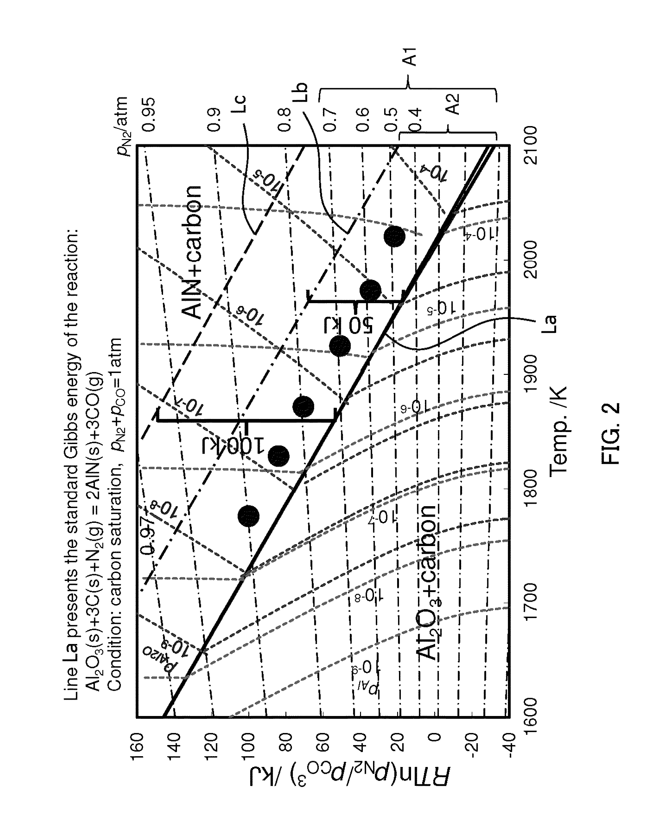
[0081]As shown in FIG. 4, the sapphire substrate was disposed in the holding furnace unit of the reaction vessel 1. First, after using a rotary pump to clear the interior of the reaction vessel 1, the N2 / CO mixed gas was introduced therein by the gas intake unit 3. T...

example 2

[0083]The AlN / sapphire substrate used herein was formed in Example 1 by MOVPE, and is one of the four equally formed pieces. Annealing was performed in Example 2 in a manner similar to Example 1 other than that the N2 / CO mixed gas ratio was set to 0.80 / 0.20, and that the annealing temperature was set to 1600° C.

[0084]As a result, the crystalline properties of the AlN layer were as follows: the FWHM of the XRC of the (0002) AlN was 97 arcsec, the FWHM of the XRC of the (10-12) AlN was 468 arcsec, and the FWHM of the XRC of the (10-10) AlN was 662 arcsec. Also, the roughness mean square (RMS) of the surface was 0.63 nm, and compared to before annealing, excellent crystalline properties and surface smoothness were seen.

example 3

[0085]The AlN / sapphire substrate used herein was formed in Example 1 by MOVPE, and is one of four equally formed pieces. Annealing was performed in Example 3 in a manner similar to Example 1 other than that the N2 / CO mixed gas ratio was set to 0.85 / 0.15, and that the annealing temperature was set to 1550° C.

[0086]As a result, the crystalline properties of the AlN layer were as follows: the FWHM of the XRC of the (0002) AlN was 43 arcsec, the FWHM of the XRC of the (10-12) AlN was 579 arcsec, and the FWHM of the XRC of the (10-10) AlN was 867 arcsec. Also, the roughness mean square (RMS) of the surface was 1.21 nm, and compared to before annealing, excellent crystalline properties and surface smoothness were seen.


PUM


Abstract

A substrate having an annealed AlN layer includes a substrate made of a material selected from among a group including sapphire, silicon carbide (SiC), and aluminum nitride (AlN), and an aluminum nitride (AlN) layer formed on the substrate and having a thickness of 100 nm or greater. The aluminum nitride layer is annealed at a prescribed annealing temperature and in a nitrogen/carbon monoxide (N2/CO) mixed gas atmosphere, and the nitrogen/carbon monoxide (N2/CO) mixed gas has a mixture ratio of N2 gas/CO gas in a range of 0.95/0.05 to 0.4/0.6.

Description

BACKGROUND OF THE INVENTION[0001]1. Technical Field[0002]The present invention relates to a substrate having an aluminum nitride (AlN) layer and a method for manufacturing an aluminum nitride (AlN) layer in which an aluminum nitride (AlN) layer is annealed in a high temperature mixed gas of nitrogen / carbon monoxide (N2 / CO) atmosphere to achieve a higher quality aluminum nitride crystalline layer (hereinafter, “AlN layer”).[0003]2. Background Art[0004]Ultraviolet light-emitting elements are garnering wide attention as next generation light sources as a replacement for fluorescent lights, for use in high density DVDs, for lasers for use in chemistry, for breaking down pollutants by photocatalysis, for use in He—Cd lasers, as a replacement for mercury lamps, and the like. Such ultraviolet light-emitting elements are made of an AlGaN nitride semiconductor known as a wide gap semiconductor, and are layered on a substrate of a different material such as sapphire.[0005]However, sapphire ha...

Claims


Application Information

Patent Timeline
IPC IPC(8): H01L33/12H01L33/32H01S5/323H01L33/00
CPCH01L33/12H01L33/007H01S2304/04H01L33/32H01S5/323H01L33/0095H01L21/0242H01L21/02458H01L21/0254H01L21/0262H01L21/02658H01L21/02664H01L33/0066H01S5/0206H01S5/32341
Inventor FUKUYAMA, HIROYUKIMIYAKE, HIDETO
Owner TOHOKU UNIV
Why Eureka
Try Eureka