Low temperature polycrystalline silicon TFT array substrate and method of producing the same, display apparatus

Active Publication Date: 2016-09-15
BOE TECH GRP CO LTD
View PDF2 Cites 8 Cited by
  • Summary
  • Abstract
  • Description
  • Claims
  • Application Information

AI Technical Summary

Benefits of technology

[0031]Preferably, in the step e), the pixel definition layer formed on the pixel electrode is formed by acrylic materials with a thickness of 1˜4 micrometers. The step e) comprises: after forming the pixel definition layer on the pixel electrode, further annealing the low temperature polycrystalline silicon field effect thin film transistor array substrate by rapid thermal annealing or heat treatment furnace annealing to stabilize the characteristics of the low temperature polycrystalline silicon field effect thin film transistor.
[0032]According to another aspect of the present disclosure, it also provides a low temperature polycrystalline silicon field effect thin film transistor array substrate produced by the method as described above.
[0033]Preferably, the gate electrode, the source electrode and the drain electrode are pr

Problems solved by technology

The organic light emitting diode has a long lifetime due to its low operation voltage and high density driving architecture.
In the conventional process for producing the low temperature polycrystalline silicon field effect thin film transistor array

Method used


Image

  • Low temperature polycrystalline silicon TFT array substrate and method of producing the same, display apparatus
  • Low temperature polycrystalline silicon TFT array substrate and method of producing the same, display apparatus
  • Low temperature polycrystalline silicon TFT array substrate and method of producing the same, display apparatus

Examples


Example

[0042]Reference Numerals: 1. Substrate; 2. Buffer layer; 3. Polycrystalline silicon storage capacitor; 4. Polycrystalline silicon active layer; 5. Photo resist; 5a, 5c. Full thickness photo resist; 5b, 5d. Half thickness photo resist; 6. Gate insulation layer; 7. Gate electrode; 7a. Gate line; 8. Interlayer insulation layer; 9. Source electrode; 9a. Source contact electrode; 9b. data line; 10. Drain electrode; 11. Passivation layer; 12. Pixel electrode; 12a. Residual pixel electrode film (Transparent conductive film); 13. Pixel definition layer; 14. Gate line connecting conductive film; 15. Source electrode contact hole; 16. Drain electrode contact hole; 17. Via hole; 18. Organic planarization layer; 19. Polycrystalline silicon film; 20. Passivation layer via hole.

DETAILED DESCRIPTION OF THE PREFERRED EMBODIMENTS

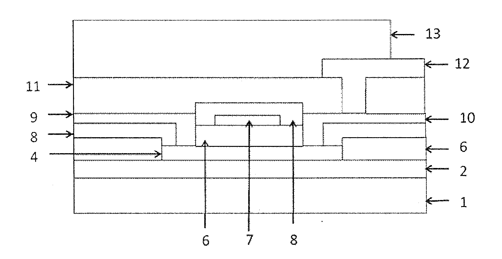
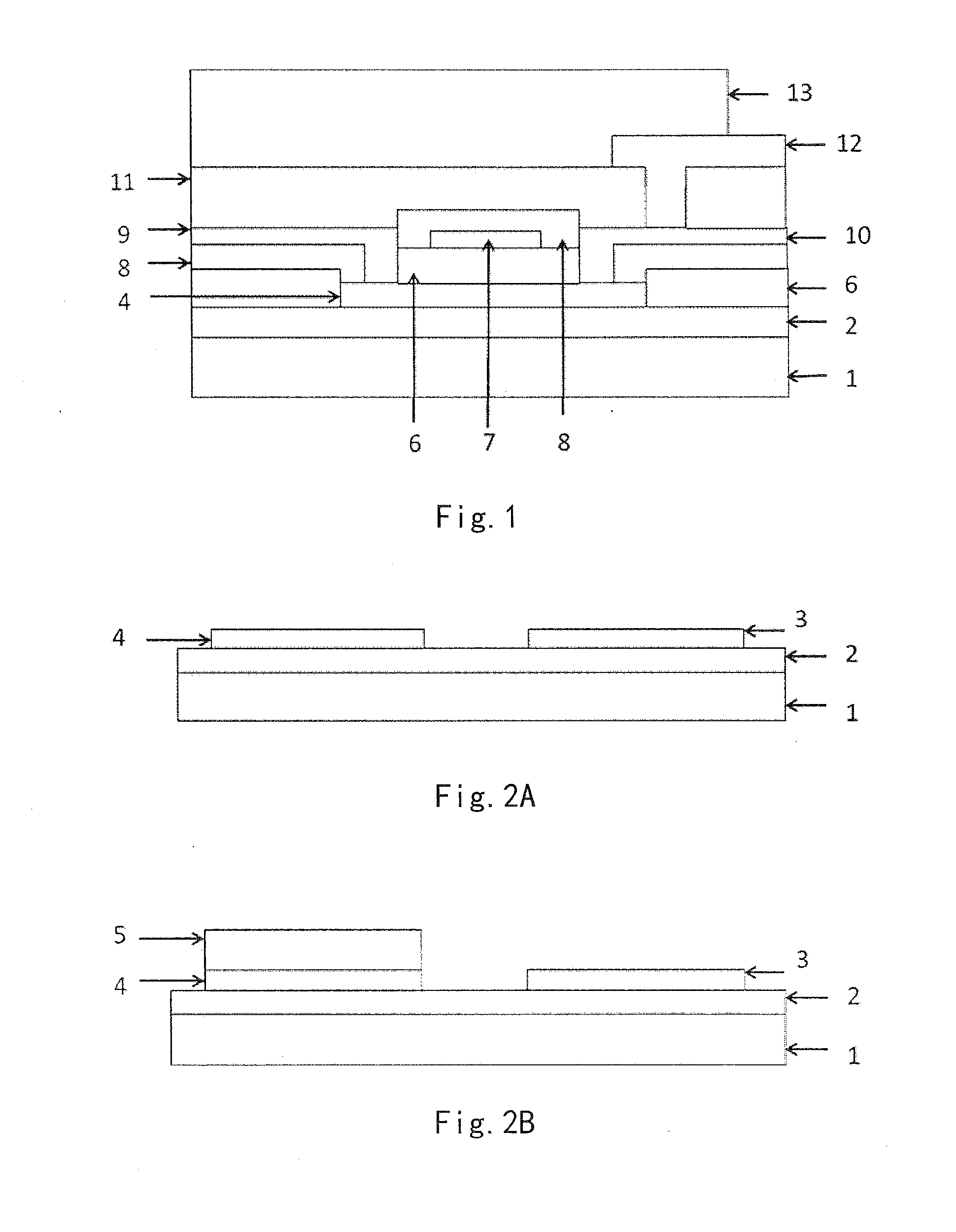
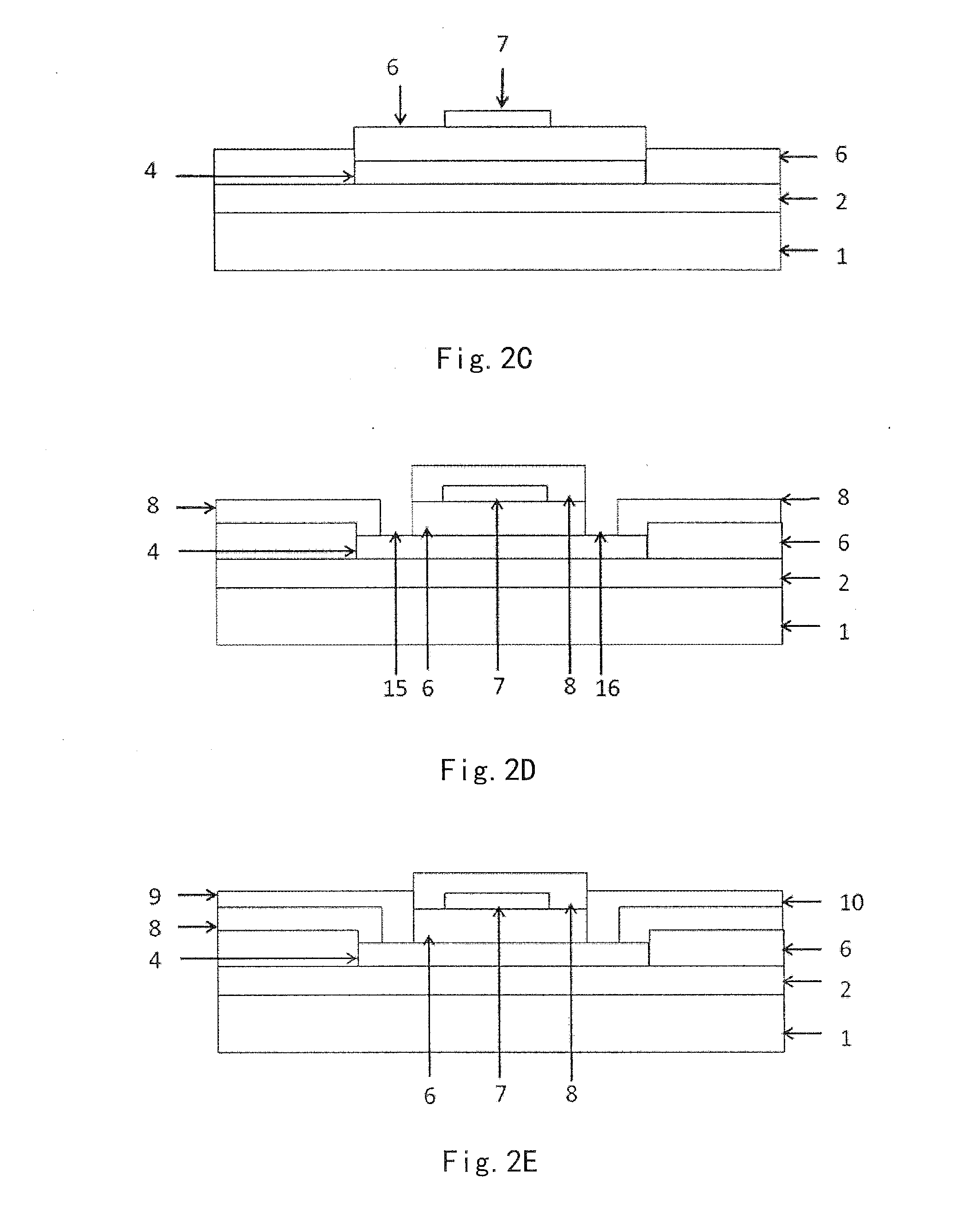
[0043]In order that objects, solutions and advantages of the present disclosure will become more apparent and explicit, the embodiments of the present disclosure will be des...


PUM


Abstract

The present disclosure provides a low temperature polycrystalline silicon field effect TFT array substrate and a method for producing the same and a display apparatus. The method: using a stepped photo resist process to form a polycrystalline silicon active layer and a lower polar plate of a polycrystalline silicon storage capacitor simultaneously on a substrate in one lithographic process; forming a gate insulation layer on the polycrystalline silicon active layer and the lower polar plate of the polycrystalline silicon storage capacitor; forming a metal layer on the gate insulation layer and etching the metal layer to form a gate electrode and gate lines connected with the gate electrode, a source electrode, a drain electrode and data lines connected with the source electrode and the drain electrode; forming a passivation layer, a photo resist layer and a pixel electrode layer in sequence and patterning the passivation layer, the photo resist layer and the pixel electrode layer to form patterns of an interlayer insulation layer via hole and a pixel electrode in one lithographic process; forming a pixel definition layer on the pixel electrode. The present disclosure may reduce times of lithographic processes for the low temperature polycrystalline silicon field effect TFT array substrate, improve the yield and reduce the costs.

Description

CROSS-REFERENCE TO RELATED APPLICATION[0001]This application claims the benefit of Chinese Patent Application No. 201410305758.6 filed on Jun. 30, 2014 in the State Intellectual Property Office of China, titled with “low temperature polycrystalline silicon TFT array substrate and method of producing the same, display apparatus”, the whole disclosure of which is incorporated herein by reference.BACKGROUND[0002]1. Field of the Disclosure[0003]The present disclosure relates to the technical field of producing an active matrix organic light emitting diode display, and in particular, to a low temperature polycrystalline silicon field effect thin film transistor (TFT) array substrate and a method of producing the same, and a display apparatus including the low temperature polycrystalline silicon field effect thin film transistor array substrate.[0004]2. Description of the Related Art[0005]In comparison with a liquid crystal display, an organic light emitting diode display has advantages o...

Claims


Application Information

Patent Timeline
IPC IPC(8): H01L27/12H01L29/786
CPCH01L27/1288H01L27/1222H01L27/124H01L2227/323H01L27/1285H01L29/78675H01L27/3262H01L27/1255H01L27/1237H10K59/1201H10K59/1213
Inventor LONG, CHUNPINGLIANG, YINANLIU, ZHENGWANG, ZUQIANGTIAN, XUEYAN
Owner BOE TECH GRP CO LTD
Why Eureka
Try Eureka