Apparatus and method for forming thin protective and optical layers on substrates

a technology of protective and optical layers, applied in the field of apparatus and methods for plasma processing, can solve the problems of not being economical for larger screens, unable to produce very thin coatings that are sometimes needed, and significant technical challenges in providing hermetic coatings or other, so as to improve improve the effect of plasma energy and gas composition control, and improve the control of deposited film properties

Inactive Publication Date: 2016-10-06
AIXTRON AG
View PDF4 Cites 45 Cited by
  • Summary
  • Abstract
  • Description
  • Claims
  • Application Information

AI Technical Summary

Benefits of technology

[0013]Enhanced process control of plasma and gas properties in plasma sources (also called linear plasma generating units—PGUs), and properties of deposited films of various types are provided herein. A plasma source is also provided having multiple plasma regions that impart improved control of plasma energy and gas composition in such regions. Such improved local control of reactive species generation and how these species interact with a substrate to be processed in proximity to the source permit superior control of deposited film properties when the substrate temperature during deposition is decreased, particularly below about 150° C. In some embodiments the radio frequency (RF) or VHF voltage from one or more power supplies is distributed to electrodes within a plasma source or PGU by adding a circuit or transformer that can insert a phase angle between the frequency components of the voltage on adjacent electrodes. The phase and distribution of frequencies—as well as the gaps between electrodes relative to their gaps to the substrate—controls the relative magnitude of plasma energy density between the electrodes versus that between electrodes and the substrate. For some implementations the cross-sectional shape of each electrode may be used to create regions of increased or reduced plasma power density. Thus, in some example embodiments regions of the plasma that are desired to have higher power density may have a closer spacing of electrodes from one side of that plasma region to either an electrode or to a passive surface (such as a grounded surface or substrate) on the opposite side. In some example embodiments the RF or VHF power signal delivered to adjacent electrodes may be pulsed with relative timing to alter the chemistry and / or spatial distribution of the plasma surrounding the electrodes.
[0015]In other inventive embodiments, an additional bias inducing electrode is positioned on the opposite side of the substrate being coated so that it increases ion bombardment power and ion energy on some part of the area of the substrate during coating. By making such a bias electrode much smaller in area than the upper electrodes it provides concentrated ion bombardment energy onto the substrate rather than onto electrodes or insulators. This additional lower electrode can be powered independently, or by the same circuit as the electrodes of the plasma source / PGU by connection to an RF or VHF supply. In embodiments where the lower electrode is separately powered the ion bombardment power for the growing substrate can be more accurately and efficiently controlled.
[0016]In other inventive embodiments, an inert or deactivating gas is injected next to a more reactive precursor. This inert or deactivating gas may either serve as a diffusion barrier reducing the reactive species concentration in the volume close to the injection point. This can help reduce undesirable deposition and build up that may occur on electrode or divider surfaces next to the precursor injection point.

Problems solved by technology

Currently, there are significant technical challenges in providing hermetic coatings or other protective layers on polymer materials, plastic substrates or sensitive inorganic materials.
Another major and challenging application is to form protective layers having very few defects or “pinholes” to cover active matrix OLED screens or lighting panels.
While liquid-based application may be cheaper to apply it often requires extensive drying / curing operations and usually cannot produce very thin coatings that are sometimes needed.
This process works well for small display but is not economical for larger screens due in large part to the limits defects introduced by the sputtering process.
This areal density of defects is not adequate even for screens as small as those for “pad” devices, let alone notebook computers where yields would be less than one good screen for per five manufactured.
Further, coatings applied using such technologies have general characteristics, strengths and limitations which make them more or less specific to each of the different types of applications.
Sputtering has been the most common type of deposition technology used for making very thin coatings at low temperature but this technology often has problems with cleanliness and can also cause excessive heating of the substrate due to the inability to remove heat from the substrate at the low reactor gas pressures required for sputtering processing.
PECVD is an alternative but has not been able to make good quality films at substrate temperatures less than about 200° C. Such systems include such as the Applied Materials cluster reactor for deposition of silicon and silicon nitride thin films in LCD screen manufacture, or in-line systems such the Roth & Rau system for coating solar cell wafers with silicon, or dielectrics such as silicon oxide.
Scaling such reactors to process ever larger substrates has made it increasingly difficult to maintain the desired film properties and uniformity of thickness of the coating across the entire substrate.
The columnar structure is not desired for barrier films since the defective region surrounding each column extends across the thickness of the film allowing for high rates of diffusion / penetration by gas or liquid.
However, the low process chamber pressure during sputtering makes it difficult to dissipate the heat added to the substrate by impinging ions.
The methods to control substrate temperature during sputtering developed for integrated circuit processing, such as electrostatic chucks and backside He flow, are not practical or economical for substrates that are large, made from dielectric materials, or continuously moving.
For example, microwave deposition systems typically produces coatings at a higher rate and more efficiently from the gas feedstock, but the coatings tend to be less dense, more tensile in film stress and may not adhere well to the underlying material.
The reason is that in sputtering systems there is no inherent tendency for particles to be captured before ending up on the substrates and in-situ cleaning methods are not as easily incorporated in to sputtering systems.
The films ending up on these shield surfaces may be come stressed and prone to flake off, causing large particle “dumps” on to the substrates.
The prior art does not provide deposition systems that can deposit dense quality encapsulation films at high-rate and low-cost with low defect density while at the same time maintaining temperatures below 100° C. There is, therefore, a need for improved processing technology to meet these needs and at the same time be compatible with high-volume production.

Method used


Image

  • Apparatus and method for forming thin protective and optical layers on substrates
  • Apparatus and method for forming thin protective and optical layers on substrates
  • Apparatus and method for forming thin protective and optical layers on substrates

Examples


Embodiment Construction

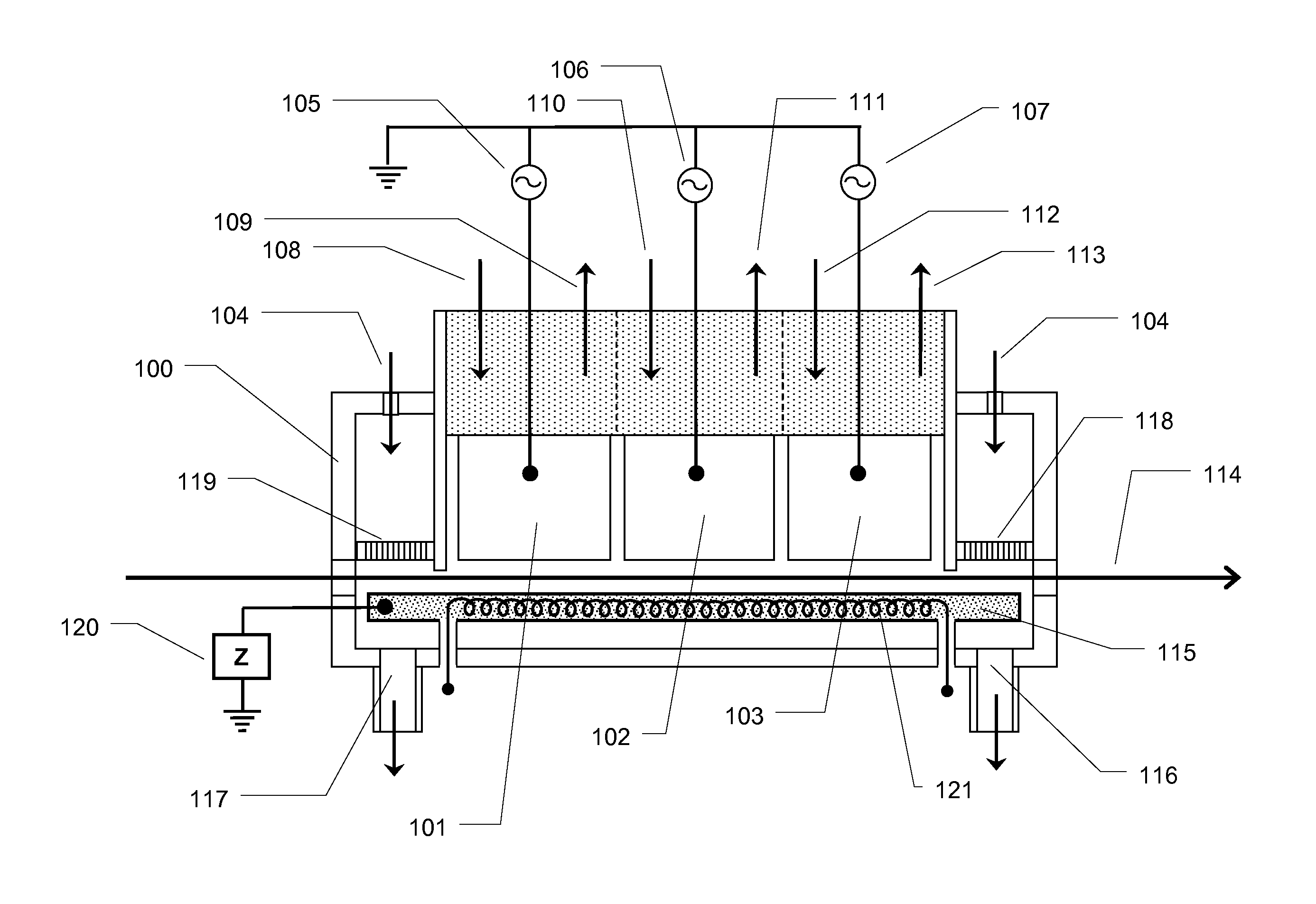
[0041]The present invention has utility in applying PECVD technology with its established benefits in low defect coatings in novel configurations that ensures the complete reaction of precursors to form high quality thin films on substrates at temperatures below 100° C. The present invention provide enhanced control of plasma properties and gas flow in the linear plasma sources, also called plasma generating units herein.

[0042]It is to be understood that in instances where a range of values are provided that the range is intended to encompass not only the end point values of the range but also intermediate values of the range as explicitly being included within the range and varying by the last significant figure of the range. By way of example, a recited range of from 1 to 4 is intended to include 1-2, 1-3, 2-4, 3-4, and 1-4.

[0043]An exemplary embodiment of a substrate processing chamber with multiple sources is shown in FIG. 1. There may be any number of sources in a processing ch...


PUM

PropertyMeasurementUnit
defect densityaaaaaaaaaa
temperatureaaaaaaaaaa

Abstract

A method and apparatus are provided for plasma-based processing of a substrate based on a plasma source having at least two adjacent electrodes positioned with the long dimensions parallel to define a first minimum gap between the two electrodes of from 5 millimeters to 40 millimeters. A second minimum gap is defined between the two electrodes and the substrate. AC power is provided to the two electrodes through separate electrical circuits from a common supply with a phase difference therebetween. A first gas and a second gas are injected into the plasma-containing volume between the two electrodes at different positions relative to the substrate. A lower electrode with a lower electrode width that is less than the combined width of the two electrodes is powered from a separately controllable AC power supply at an AC frequency different from that supplied to the two electrodes.

Description

RELATED APPLICATIONS[0001]The present application is a Divisional of U.S. patent application Ser. No. 13 / 921,969 filed Jun. 19, 2013, which is a nonprovisional of and claims priority to U.S. Provisional Application No. 61 / 661,462, filed Jun. 19, 2012, both of which are incorporated by reference herein.FIELD OF THE INVENTION[0002]The present invention in general relates to apparatus and methods for plasma processing, and in particular to alternating current powered plasma processing for ultra-clean formation of protective hermetic layers on small or large individual substrates, or large or continuous web substrates.BACKGROUND[0003]Currently, there are significant technical challenges in providing hermetic coatings or other protective layers on polymer materials, plastic substrates or sensitive inorganic materials. Some commercial applications are protective coatings for thin film photovoltaic panels, especially those having organic photovoltaic converting materials, or inorganic PV m...

Claims


Application Information

Patent Timeline
Patent Type & Authority Applications(United States)
IPC IPC(8): C23C16/509H01J37/32C23C16/458
CPCC23C16/509C23C16/458H01J2237/332H01L51/5253H01L21/0217H01J37/32568G02B1/105C23C16/545H01L21/02126H01J37/32036H01L21/02274G02B1/18G02B1/14H10K50/844
Inventor SAVAS, STEPHEN E.GALEWSKI, CARLCHATHAM, HOODMANTRIPRAGADA, SAIWIESNOSKI, ALLANJOH, SOOYUN
Owner AIXTRON AG
Why Eureka
Try Eureka