Sub-fin doped bulk fin field effect transistor (finfet), integrated circuit (IC) and method of manufacture

a field effect transistor and sub-fin doped technology, applied in the direction of transistors, semiconductor devices, electrical equipment, etc., can solve the problems of reducing the performance of the device, increasing the power consumption of the chip, and increasing the complexity of the typical fet, so as to reduce the punch-through current and reduce the effect of device performance degradation

Active Publication Date: 2016-11-10
IBM CORP
View PDF90 Cites 12 Cited by
  • Summary
  • Abstract
  • Description
  • Claims
  • Application Information

AI Technical Summary

Benefits of technology

[0015]It is yet another purpose of the invention to reduce punch-through current in bulk FinFETs without strain relaxation defects and degraded device performance.

Problems solved by technology

Thus, not withstanding the decrease of chip supply voltage, chip power consumption has increased as well.
Both at the chip and system levels, cooling and packaging costs have escalated as a natural result of this increase in chip power.
In practice however, transient power for circuit loads accounts for only a portion of the power consumed by CMOS circuits.
A typical FET is much more complex than a switch.
FETs are known, however, to conduct parasitic leakages currents, e.g., subthreshold current and punch through current.
These parasitic leakages currents result in unwanted, wasted power consumption.
In addition, gate leakages, such as gate to channel, gate to source or drain and gate induced drain leakage (GIDL), which are also related in particular to oxide thickness, contribute to static power consumption.
Multiplied by the millions, and even billions, of devices on a state of the art IC, even 100 picoAmps (100 pA) of punch through leakage current in each device, for example, can result in chip leakage on the order of 100 milliAmps (100 mA).
Thus, as chip features shrink, these parasitic leakage sources become more predominant.
Unfortunately, fin doping tends to fluctuate unacceptably.
Doping under the fins using typical state of the art ion-implantation techniques has caused device defects, especially for strained epitaxial fins such as SiGe on silicon.
These defects have caused strain relaxation that resulted in yield loss with a corresponding increase in manufacturing costs.
Moreover, a typical ion-implant can exhibit a tail that unintentionally dopes the fin channel, causing coulombic scattering that degrades channel mobility for reduced on-current flow.

Method used


Image

  • Sub-fin doped bulk fin field effect transistor (finfet), integrated circuit (IC) and method of manufacture
  • Sub-fin doped bulk fin field effect transistor (finfet), integrated circuit (IC) and method of manufacture
  • Sub-fin doped bulk fin field effect transistor (finfet), integrated circuit (IC) and method of manufacture

Examples


Embodiment Construction

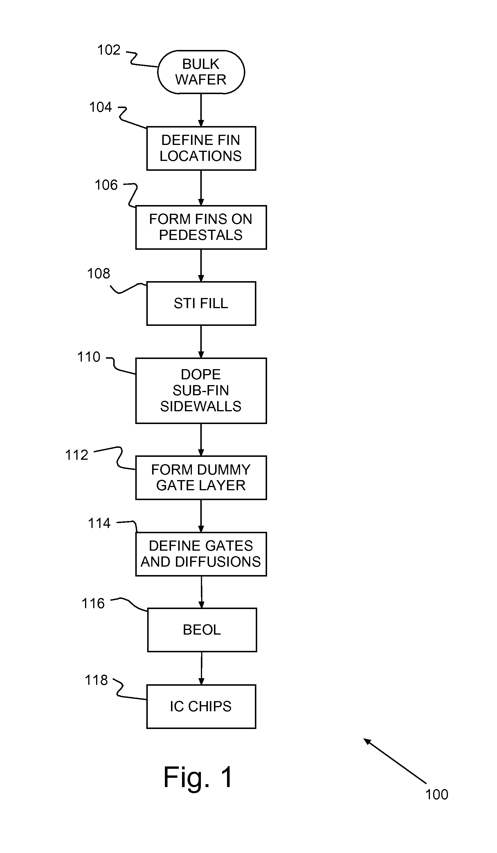
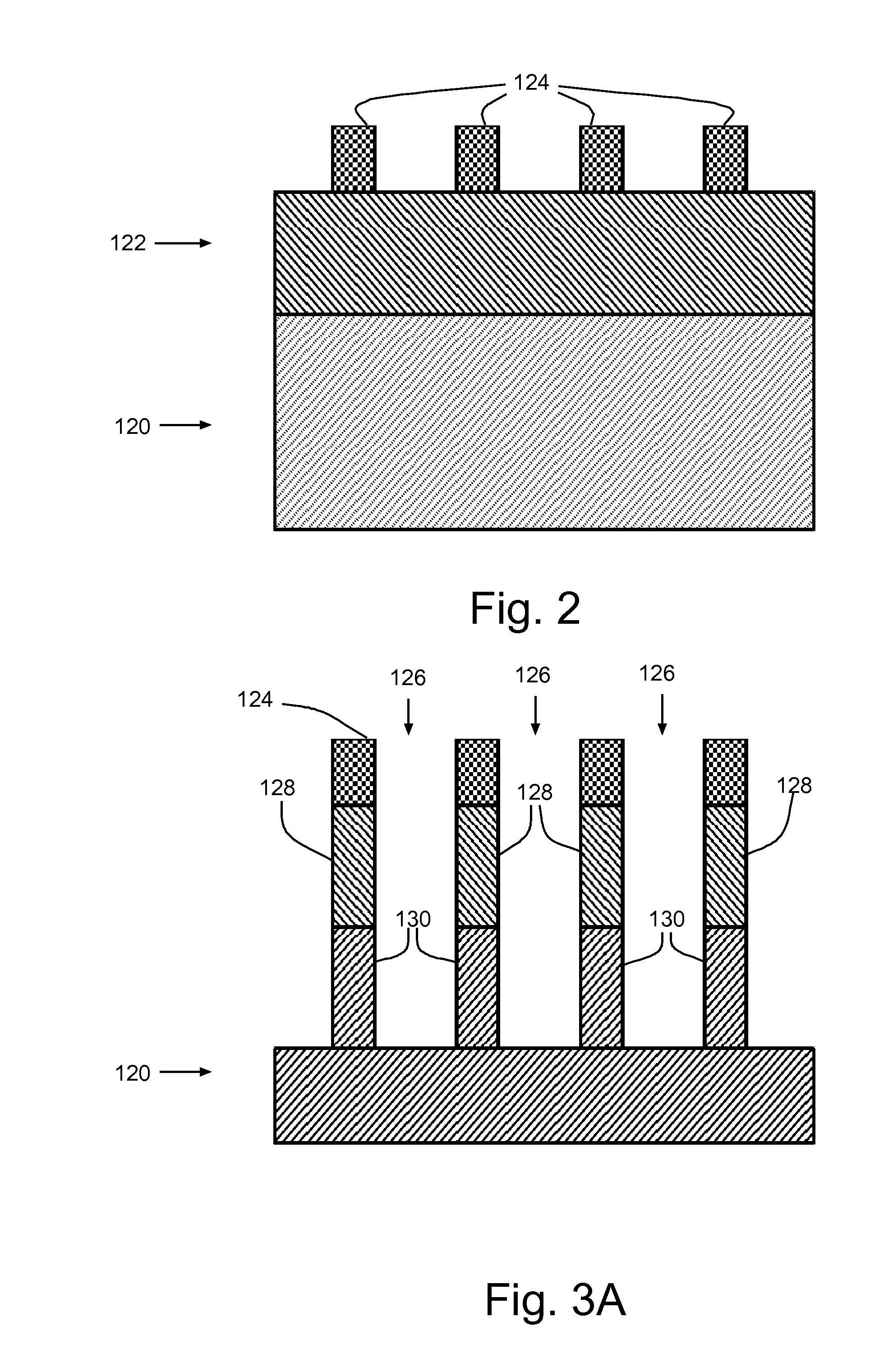
[0025]Turning now to the drawings and, more particularly, FIG. 1 shows an example of a preferred embodiment method for forming field effect transistors (FETs), e.g., in an integrated circuit (IC) and, more particularly forming FinFETs, according to the present invention. Circuit / device formation begins in step 102 with a typical bulk semiconductor wafer. In step 104 device fins are defined on a fin layer, which may be a strained layer. In step 106 fins are formed on pedestals that are formed coincidentally from the upper surface of the semiconductor wafer. Then in step 108, the space between the pedestals is filled, e.g., using a typical shallow trench isolation (STI) technique.

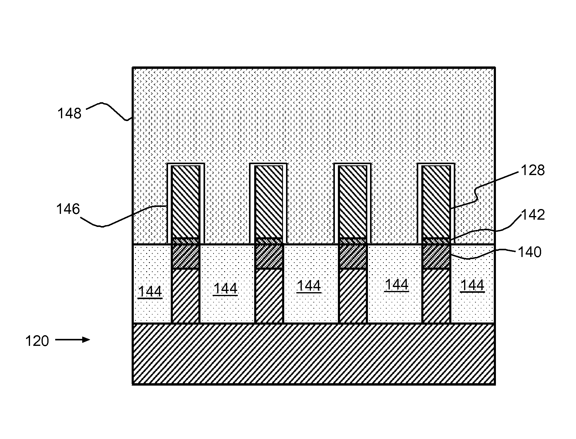
[0026]In step 110 the upper ends are the pedestals are doped without substantially doping the fins. Preferably, the STI is recessed to expose fin sidewalls. A sidewall spacer protects the fin sidewalls and the STI is further recessed, to expose the upper ends of the pedestals or sub-fins. Preferably, the expo...


PUM


Abstract

A field effect transistor (FET), integrated circuit (IC) chip including the FETs and a method of forming the IC. Fins on pedestals are defined, e.g., with a hard mask, in a fin layer on a semiconductor wafer and spaces between the pedestals are filled with dielectric material, e.g., shallow trench isolation (STI). Sacrificial sidewalls are forming along the sides of fins and pedestal sub-fins sidewalls are re-exposed. Pedestal sub-fins are doped with a punch-though dopant and punch-though dopant is diffused into the sub-fins and the bottoms of fins. After removing the hard mask and sacrificial sidewalls, metal FET gates are formed on the fins.

Description

BACKGROUND OF THE INVENTION[0001]1. Field of the Invention[0002]The present invention is related to semiconductor devices and manufacturing and more particularly to fin field effect transistors (FinFETs) formed on semiconductor wafers and methods of manufacturing Integrated Circuits (ICs) with circuits including FinFETs.[0003]2. Background Description[0004]Integrated Circuit (IC) chip density and performance are primary semiconductor technology development goals. Increased chip density (the average density of circuit transistors on a chip) and chip die size has increased the number of transistors packed on a single chip. Typically, chip density has been achieved by shrinking features sizes to pack more transistors in the same area. Another state of the art approach to increasing field effect transistor (FET) density is forming FETs vertically on narrow semiconductor surface ridges or fins. Minimum feature sized lines of semiconductor material are formed on the surface of a bulk semi...

Claims


Application Information

Patent Timeline
Patent Type & Authority Applications(United States)
IPC IPC(8): H01L27/088H01L29/167H01L21/8234H01L29/06H01L21/3105H01L21/324H01L21/308H01L21/762H01L29/66H01L29/10H01L21/223
CPCH01L27/0886H01L29/1083H01L29/167H01L21/823431H01L21/823481H01L29/0649H01L29/66803H01L21/324H01L21/3081H01L21/76224H01L29/66545H01L21/31055H01L21/223H01L21/823892H01L21/823821H01L29/785H01L29/66795
Inventor BALAKRISHNAN, KARTHIKCHENG, KANGGUOHASHEMI, POUYAREZNICEK, ALEXANDER
Owner IBM CORP
Why Eureka
Try Eureka