Wiring board with dual stiffeners and dual routing circuitries integrated together and method of making the same

Active Publication Date: 2016-12-15
BRIDGE SEMICON
View PDF18 Cites 11 Cited by
  • Summary
  • Abstract
  • Description
  • Claims
  • Application Information

AI Technical Summary

Benefits of technology

[0012]The method of making a wiring board according to the present invention has numerous advantages. For instance, inserting the sacrificial carrier and the first routing circuitry into the through opening of the first stiffener before the formation of the routing circuitry is particularly advantageous as the sacrificial carrier together with the first stiffener provides a stable platform for forming the second routing circuitry and micro-via connection failure in the subsequent formation of the sec

Problems solved by technology

However, although the inductance of these wiring boards can be reduced, other features such as design flexibility are not addr

Method used


Image

  • Wiring board with dual stiffeners and dual routing circuitries integrated together and method of making the same
  • Wiring board with dual stiffeners and dual routing circuitries integrated together and method of making the same
  • Wiring board with dual stiffeners and dual routing circuitries integrated together and method of making the same

Examples


embodiment 1

[0055]FIGS. 1-18 are schematic views showing a method of making a wiring board that includes a first stiffener, a first routing circuitry, a second routing circuitry, an array of vertical connecting channels and a second stiffener in accordance with the first embodiment of the present invention.

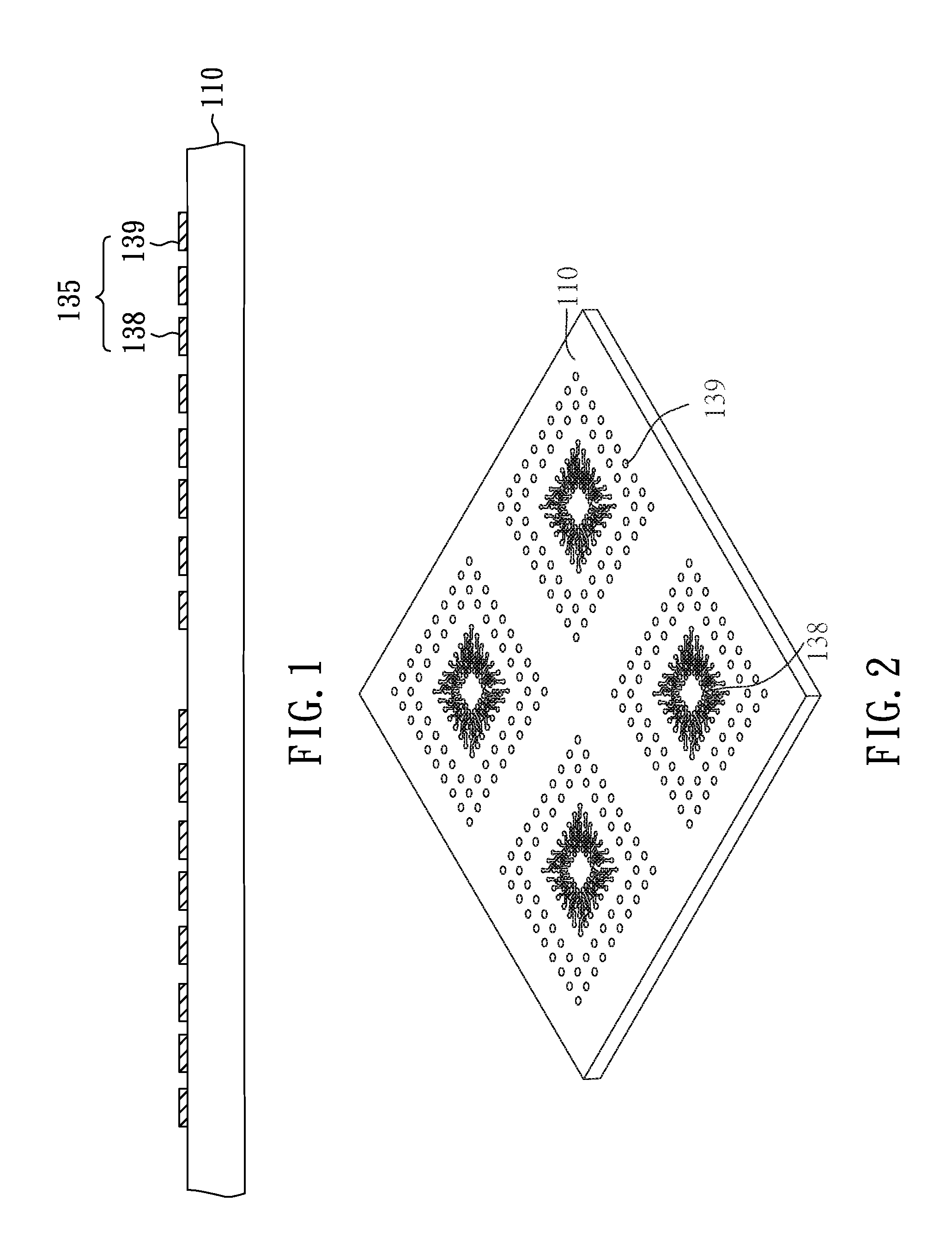
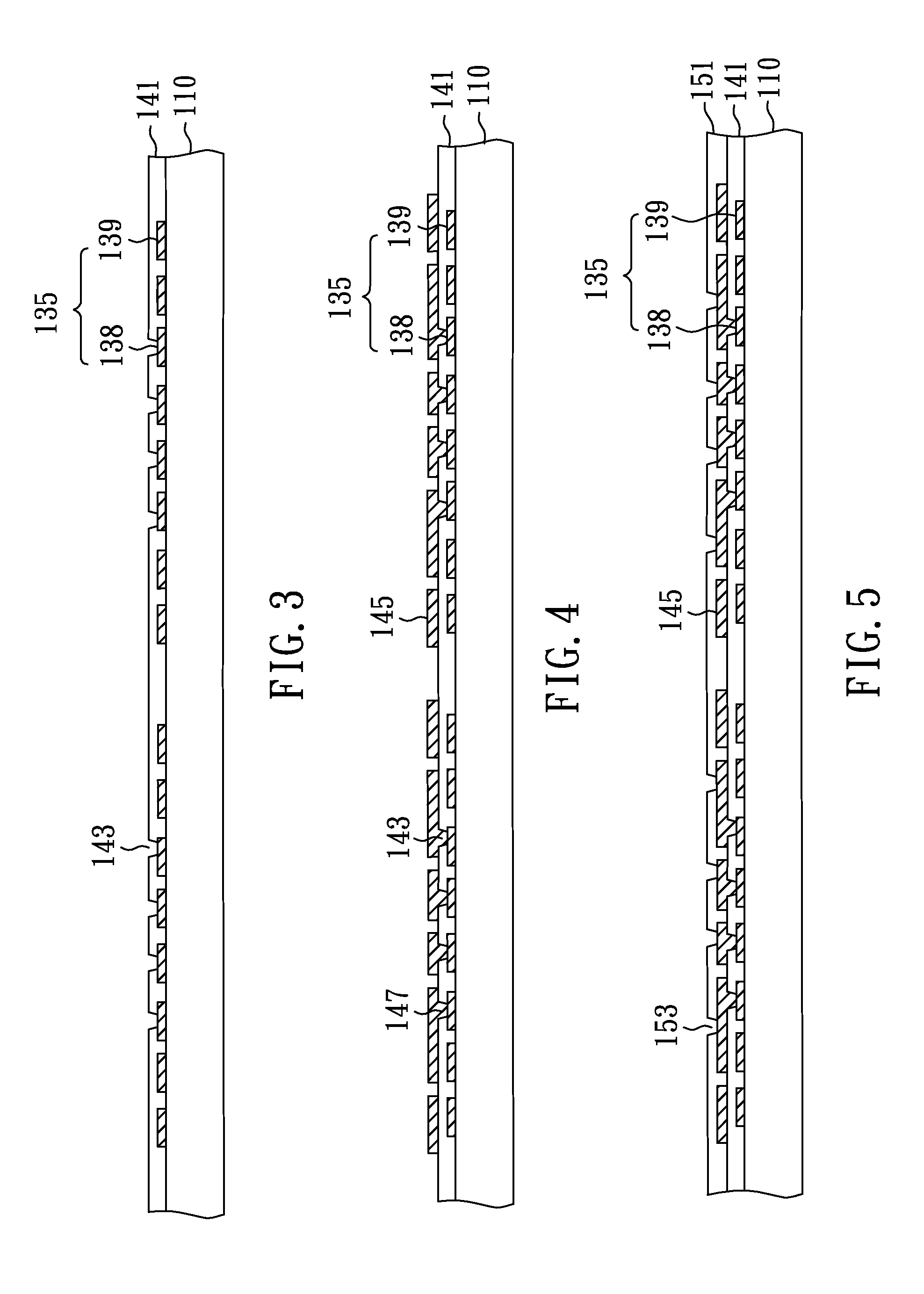
[0056]FIGS. 1 and 2 are cross-sectional and top perspective views, respectively, of the structure with routing traces 135 formed on a sacrificial carrier 110 by metal deposition and metal patterning process. In this illustration, the sacrificial carrier 110 is a single-layer structure, and the routing traces 135 include bond pads 138 and stacking pads 139. The sacrificial carrier 110 typically is made of copper, aluminum, iron, nickel, tin, stainless steel, silicon, or other metals or alloys, but any other conductive or non-conductive material also may be used. The thickness of the sacrificial carrier 110 preferably ranges from 0.1 to 2.0 mm. In this embodiment, the sacrificial carrier 110 is...

embodiment 2

[0084]FIGS. 22-31 are schematic views showing a method of making a wiring board with an electronic component encapsulated by the second stiffener in accordance with the second embodiment of the present invention.

[0085]For purposes of brevity, any description in Embodiment 1 above is incorporated herein insofar as the same is applicable, and the same description need not be repeated.

[0086]FIG. 22 is a cross-sectional view of a subcomponent 10 and a first stiffener 20 on a carrier film 30. The subcomponent 10 is similar to that illustrated in FIG. 10, except that the sacrificial carrier 110 is a double-layer structure in this embodiment. The subcomponent 10 is located within the through opening 205 of the first stiffener 20 with the sacrificial carrier 110 attached on the carrier film 30. The carrier film 30 typically is a tape and can provide temporary retention force for the subcomponent 10 steadily resided within the through opening 205. In this illustration, the subcomponent 10 an...

embodiment 3

[0101]FIGS. 34-37 are schematic views showing a method of making a wiring board with a third routing circuitry in accordance with the third embodiment of the present invention.

[0102]For purposes of brevity, any description in aforementioned Embodiments above is incorporated herein insofar as the same is applicable, and the same description need not be repeated.

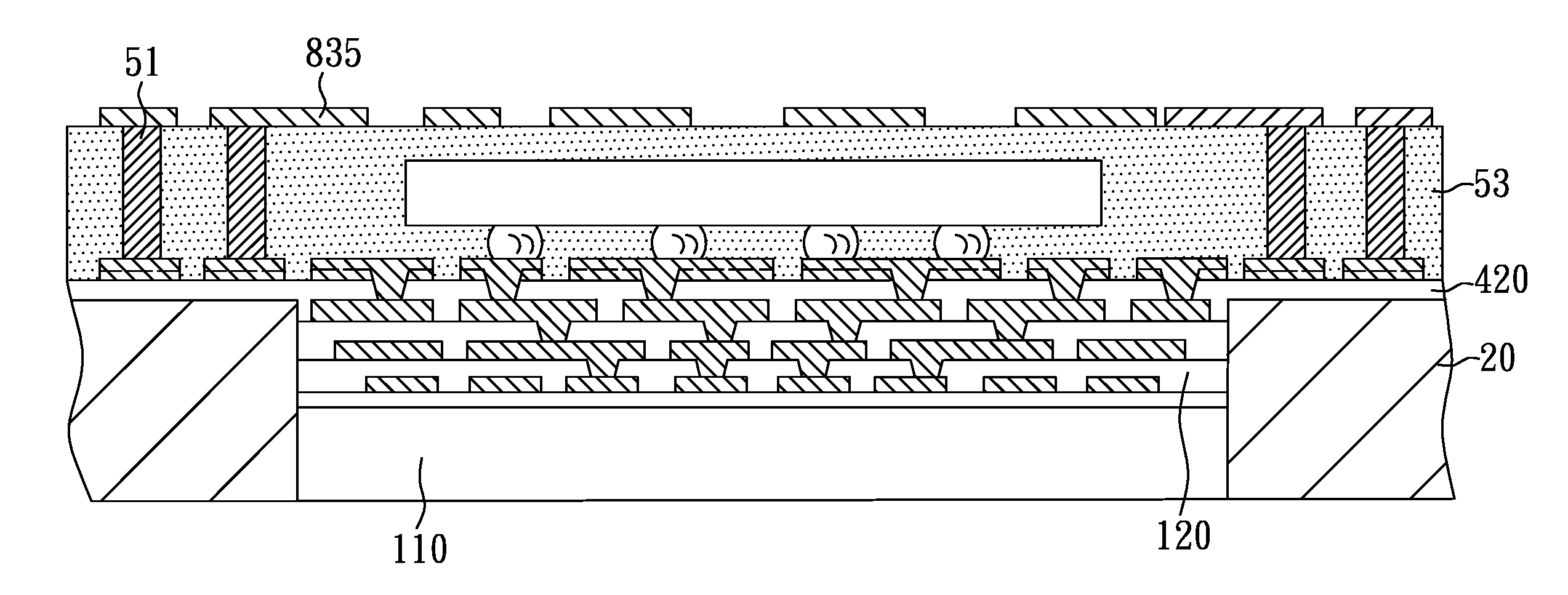
[0103]FIG. 34 is a cross-sectional view of the structure with fourth conductive traces 835 on the second stiffener 53 of FIG. 29. The fourth conductive traces 835 are formed by metal deposition and metal patterning process and laterally extend on the exterior surface of the second stiffener 53 and contact the vertical connecting channels 51.

[0104]FIG. 35 is a cross-sectional view of the structure provided with a fourth dielectric layer 841 on the second stiffener 53 as well as the fourth conductive traces 835 and fourth via openings 843 in the fourth dielectric layer 841. The fourth dielectric layer 841 is deposited typically ...


PUM


Abstract

A wiring board with dual stiffeners and integrated dual routing circuitries is characterized in that first and second routing circuitries are positioned within and beyond a through opening of a first stiffener, respectively, and an array of vertical connecting channels are disposed on the second routing circuitry and laterally surrounded by a second stiffener. The mechanical robustness of the first and second stiffeners can prevent the wiring board from warping. The vertical connecting channels can offer electrical contacts for next-level connection. The first routing circuitry, positioned within the through opening of the first stiffener, can provide primary fan-out routing, whereas the second routing circuitry not only provides further fan-out wiring structure for the first routing circuitry, but also mechanically binds the first routing circuitry with the first stiffener.

Description

CROSS REFERENCE TO RELATED APPLICATIONS[0001]This application is a continuation-in-part of U.S. application Ser. No. 14 / 746,792 filed Jun. 22, 2015, which claims the priority benefit of U.S. Provisional Application Ser. No. 62 / 092,196 filed Dec. 15, 2014 and the priority benefit of U.S. Provisional Application Ser. No. 62 / 121,450 filed Feb. 26, 2015. The entirety of each of said applications is incorporated herein by reference.FIELD OF THE INVENTION[0002]The present invention relates to a wiring board and, more particularly, to a wiring board having dual stiffeners and dual routing circuitries integrated together, and a method of making the same.DESCRIPTION OF RELATED ART[0003]Market trends of electronic devices such as multimedia devices demand for faster and slimmer designs. One of the approaches is to interconnect semiconductor chip through a coreless substrate so that the assembled device can be thinner and signal integrity can be improved. U.S. Pat. Nos. 7,851,269, 7,902,660, 7...

Claims


Application Information

Patent Timeline
IPC IPC(8): H05K1/11H05K3/46H05K3/32H05K1/18
CPCH05K1/115H05K1/185H05K1/11H05K2201/091H05K3/32H05K2201/09036H05K3/4682H01L23/49816H01L23/562H01L25/065H05K1/181H05K1/183H05K3/4694H01L2224/16225H01L2224/73204H01L23/36H01L21/486H01L23/5383H01L23/5384H01L23/5389H01L23/3128H01L2924/181H01L24/16H01L24/32H01L24/73H01L2224/16145H01L2224/32225H01L2924/00014H01L2924/15311H01L2924/15321H01L2924/3511Y02P70/50H01L2224/13099H01L2924/00012H01L2924/00
Inventor LIN, CHARLES W. C.WANG, CHIA-CHUNG
Owner BRIDGE SEMICON
Why Eureka
Try Eureka