Multi solar cell
a solar cell and multi-junction technology, applied in photovoltaic energy generation, electrical equipment, climate sustainability, etc., can solve the problems of inability to process such wafers, inability to achieve multi-junction solar cell total thickness reduction, and inability to resist residual stress
- Summary
- Abstract
- Description
- Claims
- Application Information
AI Technical Summary
Benefits of technology
Problems solved by technology
Method used
Image
Examples
first embodiment
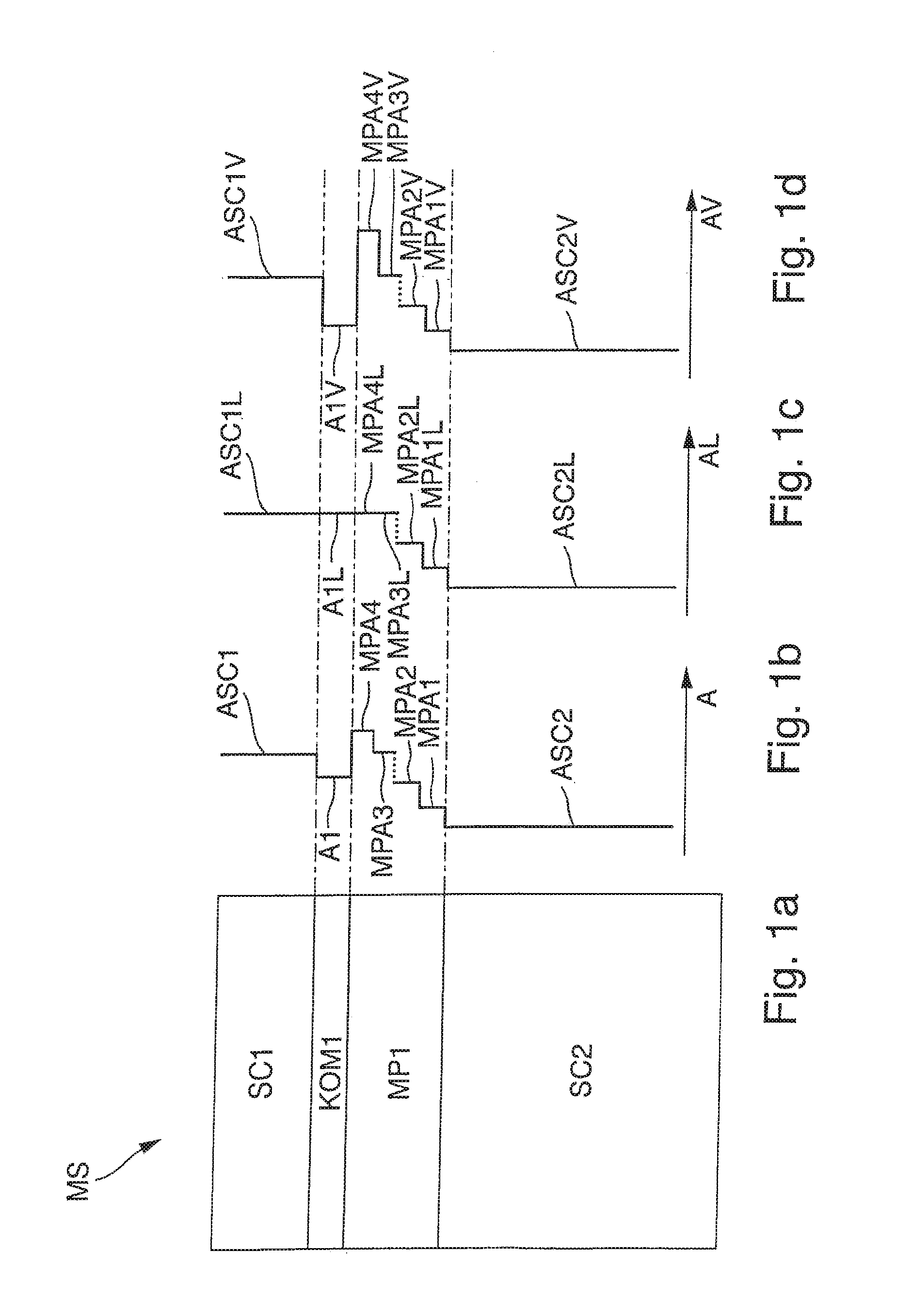
[0037]The illustration in FIG. 1a shows a cross section of the invention of a multi-junction solar cell MS with a first subcell SC1. First subcell SC1 lies on a single compensation layer KOM1. It should be noted, however, that in an alternative embodiment that is not shown, instead of a single compensation layer, a plurality of N individual compensation layers are formed. Further, compensation layer KOM1 lies on a metamorphic buffer MP1, whereby buffer MP1 lies on a second subcell SC2. The buffer has a sequence of layers that are not shown.
[0038]In the illustration in FIG. 1b, the progression of lattice constant A is plotted as a function of the layer sequence of the solar cell structure, shown in FIG. 1a. Only the differences from the illustration in FIG. 1a will be explained below. It should be noted that in the present case, lattice constant A is always understood to be the so-called natural lattice constant. Second subcell SC2 has a second lattice constant ASC2. A sequence of a ...
second embodiment
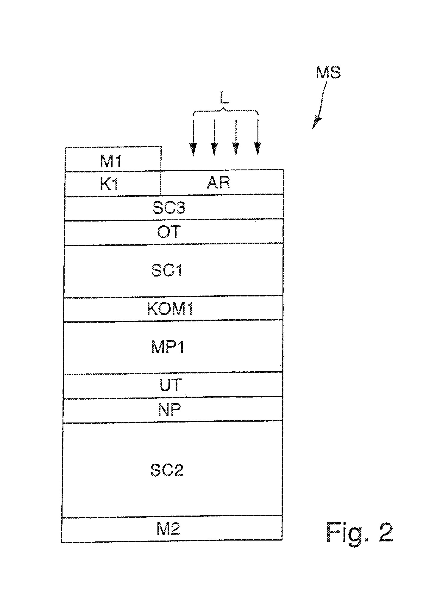
[0042]The illustration in FIG. 2 shows a cross section of the invention in the form of a triple-junction solar cell, whereby the incidence of light L occurs through an anti-reflective layer AR. Only the differences from the illustration in the previous figures will be explained below. Second subcell SC2 is preferably integrally bonded on the bottom side to a metal layer M2. Various nucleation layers and / or single buffer layers are formed between second subcell SC2 and a bottom tunnel diode UT. The upper tunnel diode OT is formed between a third subcell SC3 and between first subcell SC1. Lying on third subcell SC3 is an anti-reflective layer AR and a contact-promoting layer K1 and a first metal layer M1. Because the bottom tunnel diode UT lies under metamorphic buffer MP1, this means in this regard that a solar cell stack having an n-on-p polarity is formed and that metamorphic buffer MP1 and stress compensation layer KOM1 are positively doped. It is preferred to make the triple-junc...
third embodiment
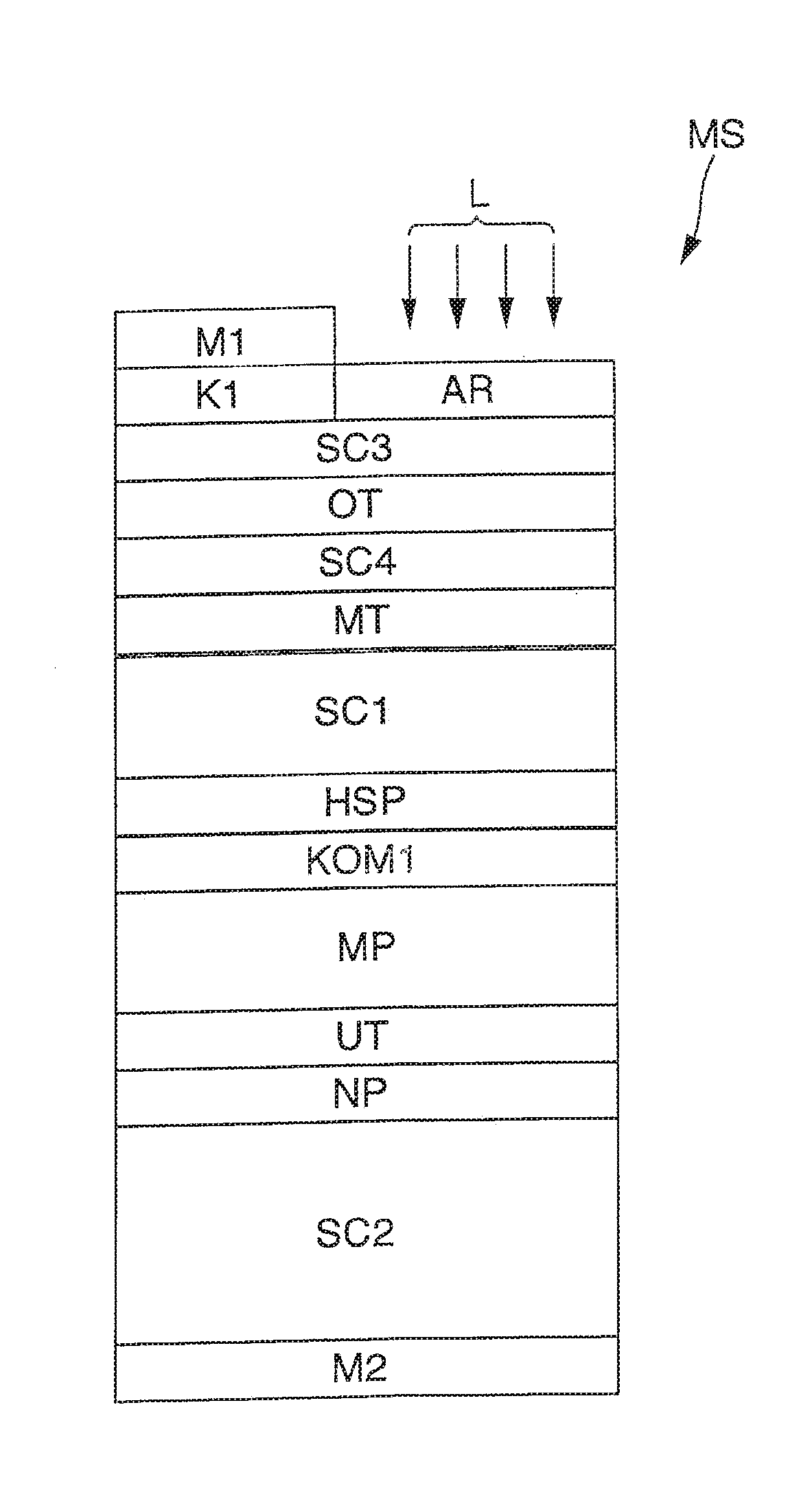
[0043]The illustration in FIG. 3 shows a cross section of the invention in the form of a quadruple-junction solar cell. Only the differences from the illustrations in the previous figures will be explained below. Preferably, the quadruple-junction solar cell comprises a compound sequence of AlGaInP / AlGaInAs / GaInAs / Ge, whereby the AlGaInP compound is arranged as the topmost subcell facing the incident light L. A semiconductor mirror HSP is formed between first subcell SC1 and compensation layer KOM1. Further, a middle tunnel diode MT is formed between first subcell SC1 and fourth subcell SC4. Furthermore, a fourth subcell SC4 is formed between first subcell SC1 and third subcell SC3.
PUM
 Abstract
Description
Claims
Application Information


