Photoelectric conversion element
a conversion element and photoelectric technology, applied in the field of photoelectric conversion elements, can solve the problems of low photoelectric conversion efficiency, and low efficiency of two-step light absorption through quantum levels (including superlattice minibands) to achieve the effect of increasing the photoelectric conversion efficiency of a photoelectric conversion elemen
- Summary
- Abstract
- Description
- Claims
- Application Information
AI Technical Summary
Benefits of technology
Problems solved by technology
Method used
Image
Examples
embodiment
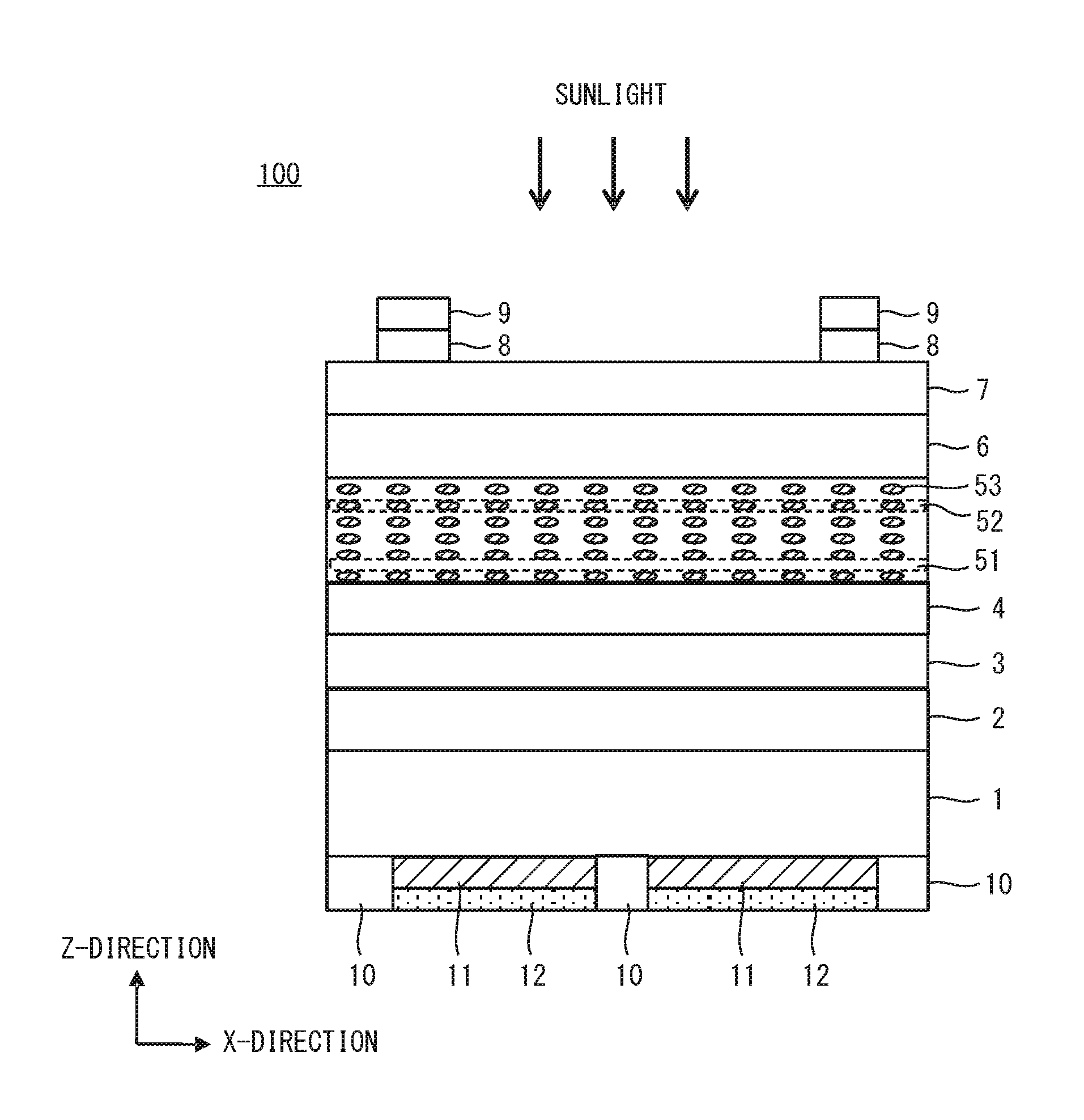
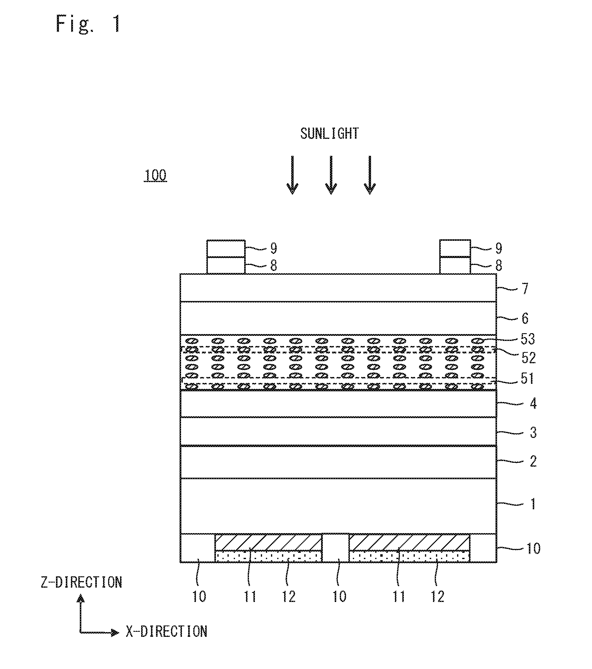
[0040]The photoelectric conversion element and a solar cell are described below in detail with reference to the attached drawings. In the drawings, the same reference numerals denote the same components or corresponding components. Dimensions such as length, width, thickness, and depth are appropriately modified for the clarification and simplification of the drawings and do not express actual dimensions.
[0041]Terms used in this specification are simply described below. The terms are used to describe a configuration in this embodiment and do not limit the present disclosure.
[0042]The term “superlattice semiconductor layer” refers to a layer having a superlattice structure composed of barrier sub-layers and quantum sub-layers alternately stacked. The barrier sub-layers and the quantum sub-layers are made of a compound semiconductor material. The barrier sub-layers are higher in band gap energy than the quantum sub-layers.
[0043]The term “quantum sub-layers” includes quantum dot sub-la...
experiment example 1
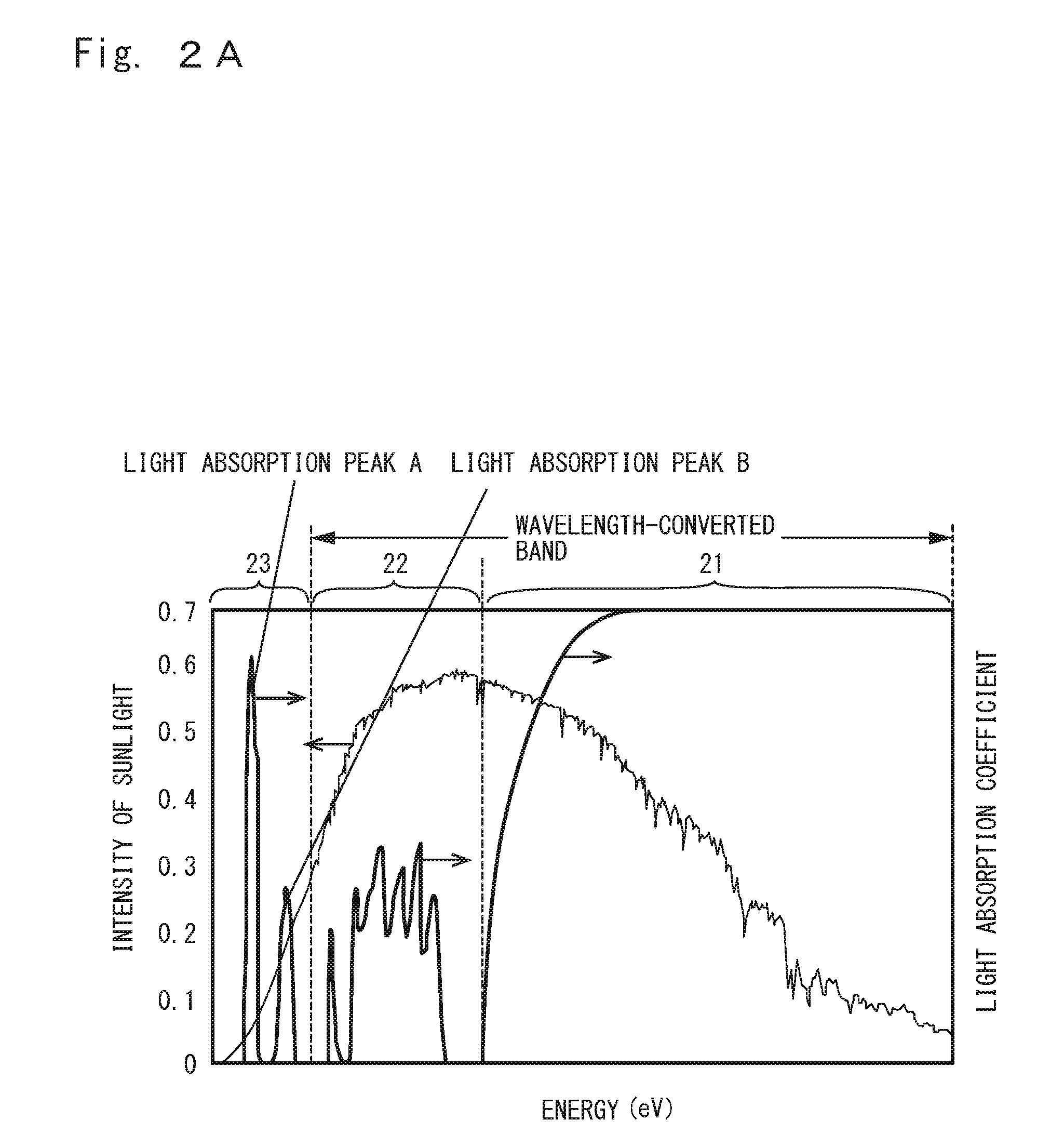
[0111]A simulation experiment below was performed using the solar cell 100 manufactured in the above embodiment.
experiment example 2
[0125]In Experiment Example 2, simulation was performed by substantially the same method as that described in Experiment Example 1 except that the height of quantum dots 53 was changed. That is, the height of the quantum dots 53 was changed from the conditions described in Experiment Example 1.
[0126]As is the case with Experiment Example 1, in a superlattice semiconductor layer 5, a base semiconductor material used to form barrier sub-layers 51 was gallium arsenide (GaAs) and a material used to form quantum dots 53 was Indium arsenide (InAs). In this experiment example, the base semiconductor material was GaAs and the material used to form the quantum dots 53 was InAsx However, a mixed crystal material such as InGaAs or a different semiconductor material may be used.
[0127]In the superlattice semiconductor layer 5, the quantum dots 53 were lens-shaped and each included a wetting layer with a thickness of about 0.5 nm, the diameter of the quantum dots 53 in the in-plane direction was ...
PUM
 Abstract
Description
Claims
Application Information


