Package-on-package semiconductor assembly having bottom device confined by dielectric recess

a semiconductor assembly and dielectric recess technology, applied in semiconductor devices, semiconductor/solid-state device details, electrical apparatus, etc., can solve the problems of significant thermal, electrical and reliability challenges in the semiconductor package industry, shortening between neighboring connections, and many deficiencies, so as to reduce the minimum required height of metal posts

Inactive Publication Date: 2017-02-02
BRIDGE SEMICON
View PDF2 Cites 20 Cited by
  • Summary
  • Abstract
  • Description
  • Claims
  • Application Information

AI Technical Summary

Benefits of technology

[0006]A primary objective of the present invention is to provide a package-on-package semiconductor assembly having a bottom device laterally confined by a recess of a dielectric layer so that the displacement of the embedded bottom device can be controlled.
[0007]Another objective of the present invention is to provide a package-on-package semiconductor assembly having an array of metal posts formed in a core base for vertical interconnection. As both the recess and the metal posts originated from a same metal carrier, the pre-determined relative location between the metal posts and the embedded bottom device can be guaranteed.
[0008]Yet another objective of the present invention is to provide a package-on-package semiconductor assembly having both the recess and the metal posts enclosed in the core base. As the minimal height of the metal posts needed for the vertical connection between opposite sides of the core base can be compensated for by the amount equal to the depth of the recess, the manufacturing yield and cost can be greatly improved.
[0010]The package-on-package semiconductor assemblies according to the present invention have numerous advantages. For instance, inserting the first semiconductor device into the recess of the dielectric layer can reduce the minimal required height of the metal posts by the amount equal to the depth of the recess of the dielectric layer. Forming the metal posts over the top surface of the dielectric layer can offer vertical routing to proceed with package-on-package interconnection procedure for the second semiconductor device disposed over the top surface of the core base and electrically coupled to the first semiconductor device through the bottom buildup circuitry.

Problems solved by technology

The convergence of mobility, communication, and computing has created significant thermal, electrical and reliability challenges to the semiconductor package industry.
Despite numerous package-on-package assemblies reported in the literature, many deficiencies remain.
As a result, these vertical channel approaches present a crowding problem that can cause shorting between neighboring connections.
Another significant drawback arising from the fabrication of the above assemblies is that the embedded / bottom device may dislocate during encapsulation or lamination.
Incomplete metallization of micro-vias due to device dislocation as described in U.S. Pat. No. 8,501,544 further degrades the quality of the electrical connection, thereby lowering the reliability and production yield of the fabricated assembly.

Method used


Image

  • Package-on-package semiconductor assembly having bottom device confined by dielectric recess
  • Package-on-package semiconductor assembly having bottom device confined by dielectric recess
  • Package-on-package semiconductor assembly having bottom device confined by dielectric recess

Examples


embodiment 1

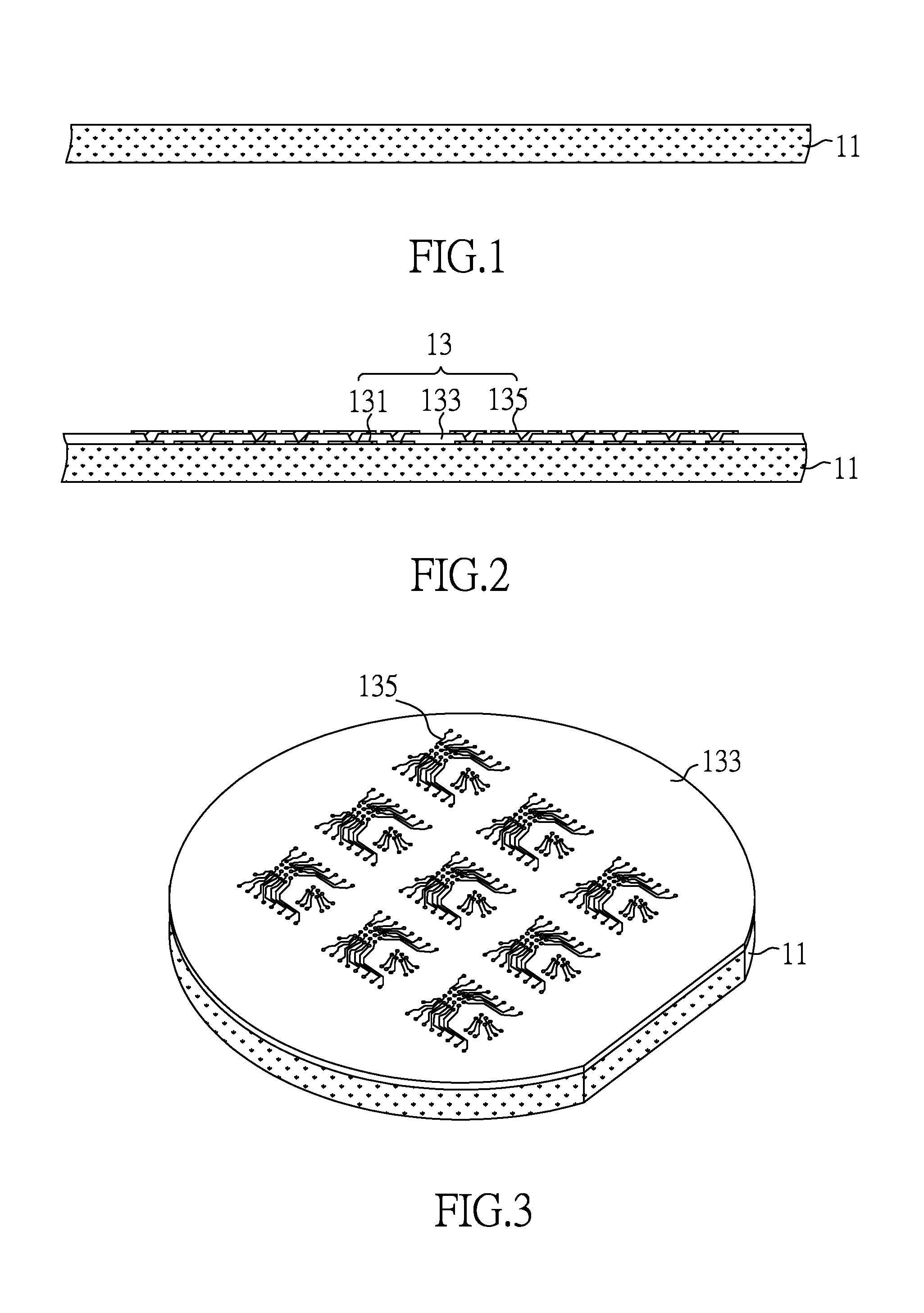
[0056]FIGS. 1-28 are schematic views showing a method of making a package-on-package semiconductor assembly that includes a first semiconductor device, a core base, a top buildup circuitry, a bottom buildup circuitry and a second semiconductor device in accordance with the first embodiment of the present invention.

[0057]FIG. 1 is a cross-sectional view of a sacrificial carrier 11. The sacrificial carrier 11 can be made of any peelable or removable material, such as silicon, copper, aluminum, iron, nickel, tin or alloys thereof.

[0058]FIGS. 2 and 3 are cross-sectional and top perspective views, respectively, of the structure with a re-distribution layer 13 formed on the sacrificial carrier 11. In this illustration, the re-distribution layer 13 includes first routing traces 131, an insulating layer 133 and second routing traces 135. The first routing traces 131 extend laterally on the sacrificial carrier 11. The insulating layer 133 contacts and covers and extends laterally on the sacr...

embodiment 2

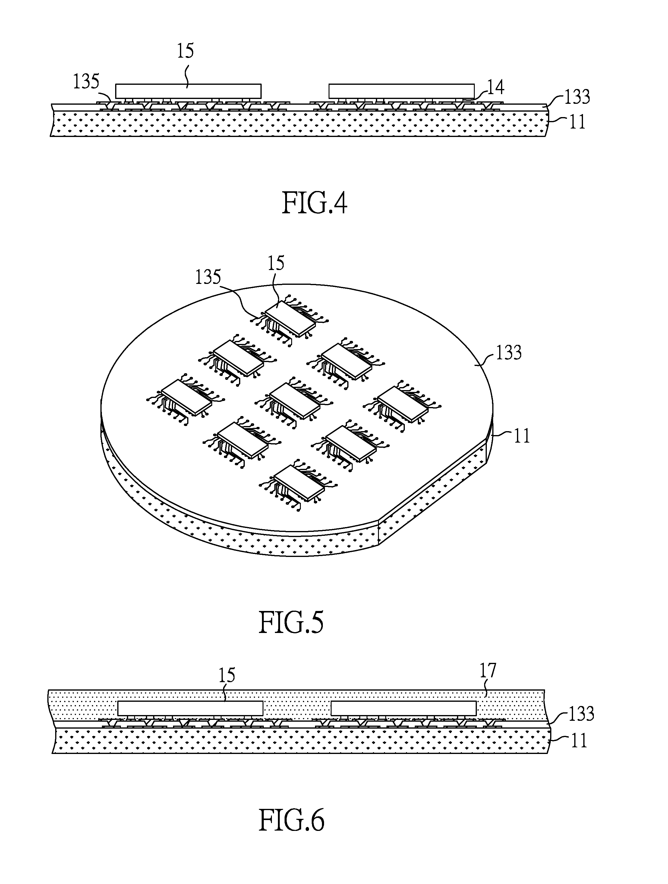
[0081]FIGS. 29-40 are schematic views showing a method of making a package-on-package semiconductor assembly with auxiliary metal pads underneath the metal posts in accordance with the second embodiment of the present invention.

[0082]For purposes of brevity, any description in Embodiment 1 above is incorporated herein insofar as the same is applicable, and the same description need not be repeated.

[0083]FIG. 29 is a cross-sectional view of the structure with a protruded metal platform 221 and an array of auxiliary metal pads 223 formed on a metal carrier 21. The protruded metal platform 221 and the auxiliary metal pads 223 extend from the bottom surface of the metal carrier 21 in the downward direction. In this illustration, the auxiliary metal pads 223 are substantially coplanar with the protruded metal platform 221 at their top and bottom surfaces. The auxiliary metal pads 223 can be made of the same material as the protruded metal platform 221, and may be formed by pattern deposi...

embodiment 3

[0097]FIGS. 41-48 are schematic views showing a method of making a package-on-package semiconductor assembly in which the first semiconductor device 10 includes protruded bumps 18 extending through the first dielectric layer 23 in accordance with the third embodiment of the present invention.

[0098]For purposes of brevity, any description in aforementioned Embodiments above is incorporated herein insofar as the same is applicable, and the same description need not be repeated.

[0099]FIG. 41 is a cross-sectional view of the structure with an array of metal posts 213 on a first dielectric layer 23. This structure can be fabricated by removing selected portions of the metal carrier 21 and the protruded metal platform 221 illustrated in FIG. 13. As a result, the first dielectric layer 23 has a recess 230 that extends from a top surface thereof, and the metal posts 213 are positioned beyond the recess230.

[0100]FIG. 42 is a cross-sectional view of the structure provided with an array of thr...


PUM


Abstract

A package-on-package semiconductor assembly is characterized by a semiconductor device positioned in a dielectric recess of a core base and surrounded by an array of metal posts. The recess in the core provides lateral displacement control between the device and the metal posts, and the minimal height of the metal posts needed for the vertical connection between two both opposite sides of the core base can be reduced by the amount equal to the depth of the recess. Further, another semiconductor device is disposed over a top surface of the core base and is electrically coupled to the semiconductor device in the dielectric recess through a buildup circuitry under a bottom surface of the core base.

Description

CROSS REFERENCE TO RELATED APPLICATIONS[0001]This application is a continuation-in-part of U.S. application Ser. No. 14 / 957,954 filed Dec. 3, 2015. This application also claims the benefit of filing date of U.S. Provisional Application Ser. No. 62 / 198,058 filed Jul. 28, 2015. The entirety of each of said applications is incorporated herein by reference.FIELD OF THE INVENTION[0002]The present invention relates to a package-on-package semiconductor assembly, more particularly, to a package-on-package semiconductor assembly having a bottom device confined by a recess of a dielectric layer and surrounded by an array of metal posts.DESCRIPTION OF RELATED ART[0003]The convergence of mobility, communication, and computing has created significant thermal, electrical and reliability challenges to the semiconductor package industry. Despite numerous package-on-package assemblies reported in the literature, many deficiencies remain. For example, the package-on-package assemblies disclosed in U...

Claims


Application Information

Patent Timeline
Patent Type & Authority Applications(United States)
IPC IPC(8): H01L25/065H01L23/528H01L23/538H01L23/31H01L23/498H01L23/00
CPCH01L25/0657H01L23/49838H01L23/49827H01L24/32H01L23/5389H01L2225/06555H01L23/528H01L2225/06548H01L2224/32225H01L2924/15153H01L23/3142H01L23/13H01L23/49816H01L2224/16235H01L2224/16238H01L2224/81005H01L2224/97H01L2924/15311H01L2924/15313H01L23/49811H01L21/561H01L25/117H01L2924/00014H01L2224/81H01L2224/13099
Inventor LIN, CHARLES W. C.WANG, CHIA-CHUNG
Owner BRIDGE SEMICON
Why Eureka
Try Eureka