

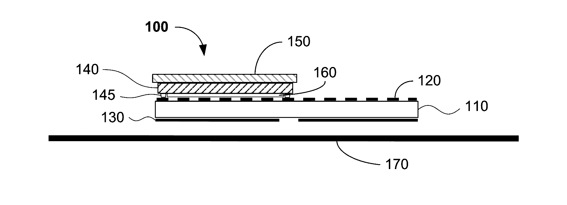
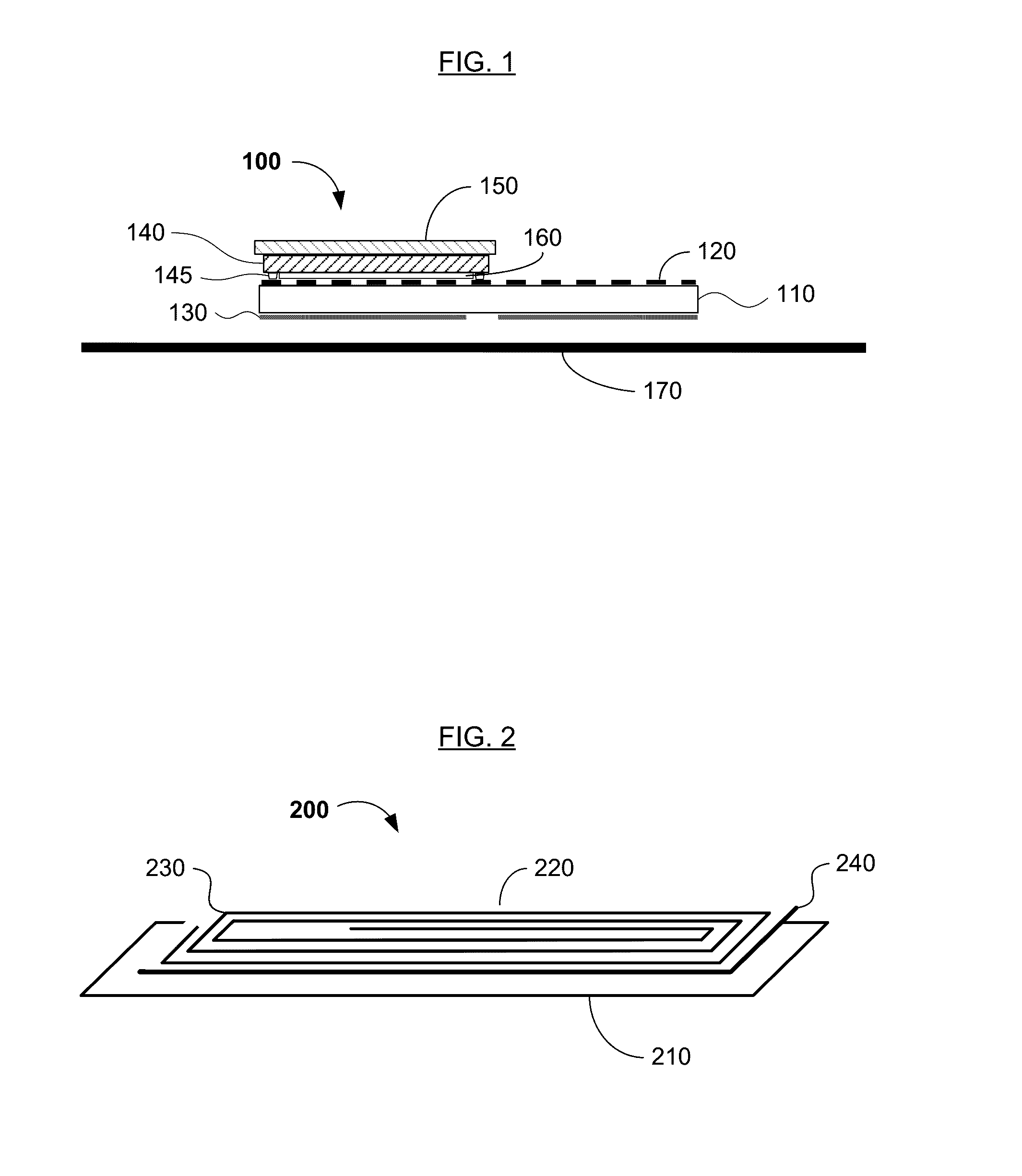
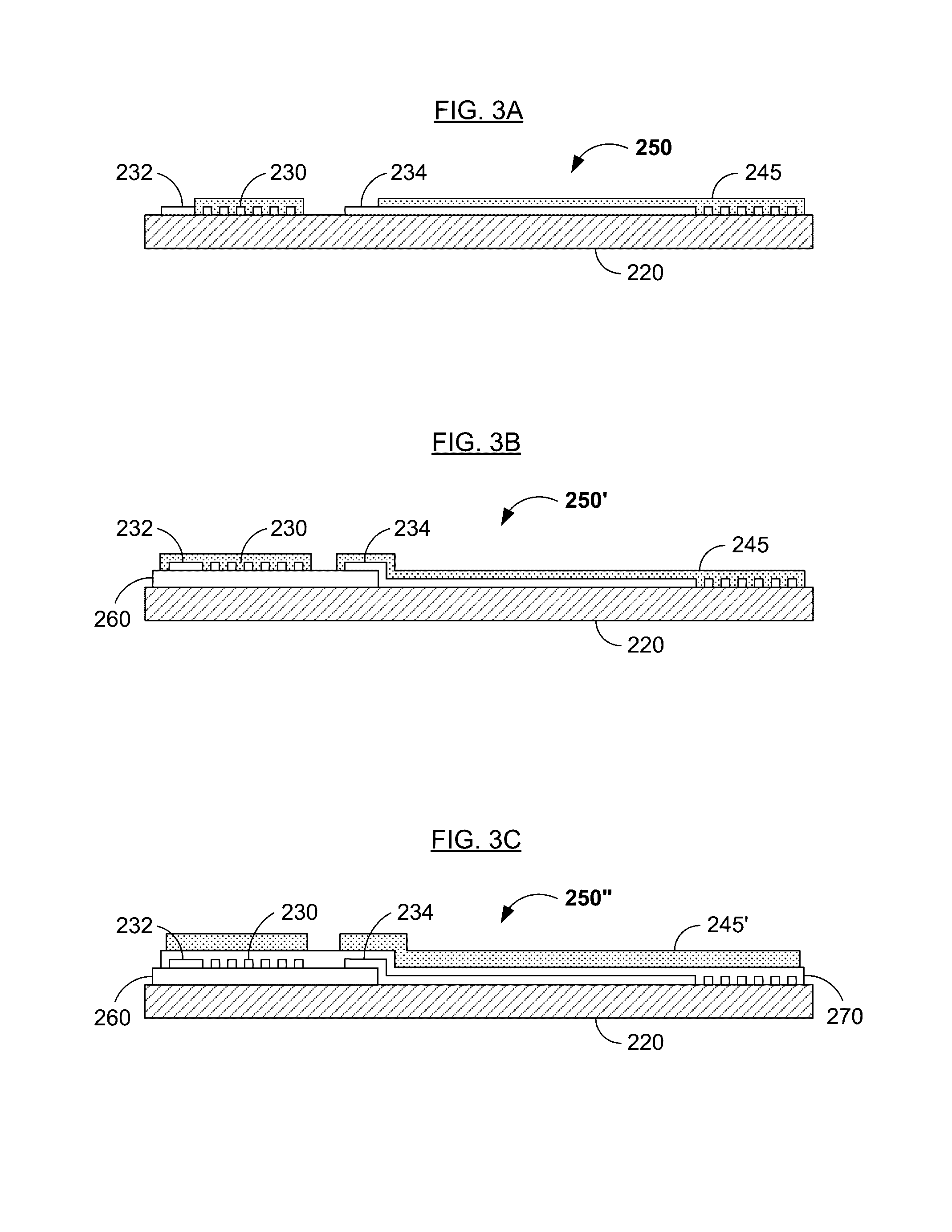
Wireless Communication Device with Integrated Ferrite Shield and Antenna, and Methods of Manufacturing the Same
a technology of ferrite shield and wireless communication, which is applied in the direction of antenna details, antenna couplings, antennas, etc., can solve the problems of poor tag read range, performance degradation of wireless tags and readers operating in the very-high frequency (vhf) system and/or communicating using magnetic couplings or magnetically coupled transponders (e, nfc) devices, etc., to achieve sufficient shielding, sufficient flexibility for application, and minimal cost
- Summary
- Abstract
- Description
- Claims
- Application Information
AI Technical Summary
Benefits of technology
Problems solved by technology
Method used
Image

Examples
experiment 1
Preparation of Polyester (Baseline) Binder Solution (20 wt %)
[0072]19 parts by weight of polyester SP185 to 1 part by weight of polyester TP220 (both of which are available from Nippon Synthetic Chemical Industry Co., Ltd., Osaka, Japan) were placed into a clean glass jar. 64 parts by weight of xylenes and 16 parts by weight of MEK were placed separately into the same jar with a magnetic stir bar, and the polyesters were dissolved in the solvents by mixing or stirring overnight. The solution is clear when the polyesters are completely dissolved. The viscosity of the polyester binder solution is 1000 cPs±50cPs.
experiment 2
Preparation of Polytetrafluoroethylene (PTFE) Binder Paste and Ferrite Paste Including the Same
[0073]1 part by weight of PTFE polymer was weighed into an aluminum weighing pan. In addition, 1.0 part by weight of a hardener was weighed in to the same weighing pan. The polymer and hardener were transferred to a jar, and 2.0 parts by weight of acetone was added. Additional acetone may be added, if necessary or desired, to extend the incubation or working time. The amount of acetone is not a factor in the final volume (ml) of paste. Using a small spatula, the paste was mixed thoroughly and additional acetone was used, if necessary or desired. To make the ferrite-containing paste, 4 parts by weight of ferrite powder was added to the mixture of PTFE and hardener in acetone and mixed further with the spatula until consistent.
experiment 3
Preparation of Polydimethylsiloxane (PDMS) Solution
[0074]10 parts by weight of PDMS was added to a clean glass jar. 40 parts by weight of xylene was added separately into the same jar to dissolve the PDMS. A magnetic stir bar was placed in the solvent / polyester mixture and stirred overnight until the solution became a single phase. When the solution is uniform, the solution is translucent and has an even flow.
PUM
 Abstract
Description
Claims
Application Information