Method of preparing a plan-view transmission electron microscope sample used in an integrated circuit analysis

a technology of transmission electron microscope and integrated circuit, which is applied in the direction of sampling, instruments, electric discharge tubes, etc., can solve the problems of large amount of region on the chip being completely removed, subsequence analysis difficult to perform or could not be performed at all, etc., to reduce the difficulty of sample preparation and analysis cost, and improve analysis efficiency and quality

Active Publication Date: 2017-02-23
SHANGHAI HUALI MICROELECTRONICS CORP
View PDF22 Cites 3 Cited by
  • Summary
  • Abstract
  • Description
  • Claims
  • Application Information

AI Technical Summary

Benefits of technology

[0031]It can be seen from the above technical solution, the present invention cuts out TEM sample only in the target region without causing the rest chip being severely damaged, by using the carrying slice as a transition medium, which is very suitable for cases have multiple analysis targets with limited number of chips, such as reverse engineering. The present invention can prepare the plan-view TEM samples conveniently, and most importantly, this method can prevent the rest of chip from being severely damaged so as to provide good condition for the subsequent various analyses; and this method can reduce the difficulty of the sample preparation and the analysis cost, and it is very effective to improve the analysis efficiency and quality.

Problems solved by technology

However, the first step of the above process of preparing the plan-view TEM sample needs to cleave or polish the sample to an extent that the cross section of the sample is close to the target region, and this step will cause a large amount of region on the chip be completely removed, which will cause subsequence analyses difficult to perform or could not perform at all.
Therefore, how to obtain the planar TEM data in the target region while the rest of chip is not damaged, is a new challenge for people in this field.

Method used


Image

  • Method of preparing a plan-view transmission electron microscope sample used in an integrated circuit analysis
  • Method of preparing a plan-view transmission electron microscope sample used in an integrated circuit analysis
  • Method of preparing a plan-view transmission electron microscope sample used in an integrated circuit analysis

Examples


Embodiment Construction

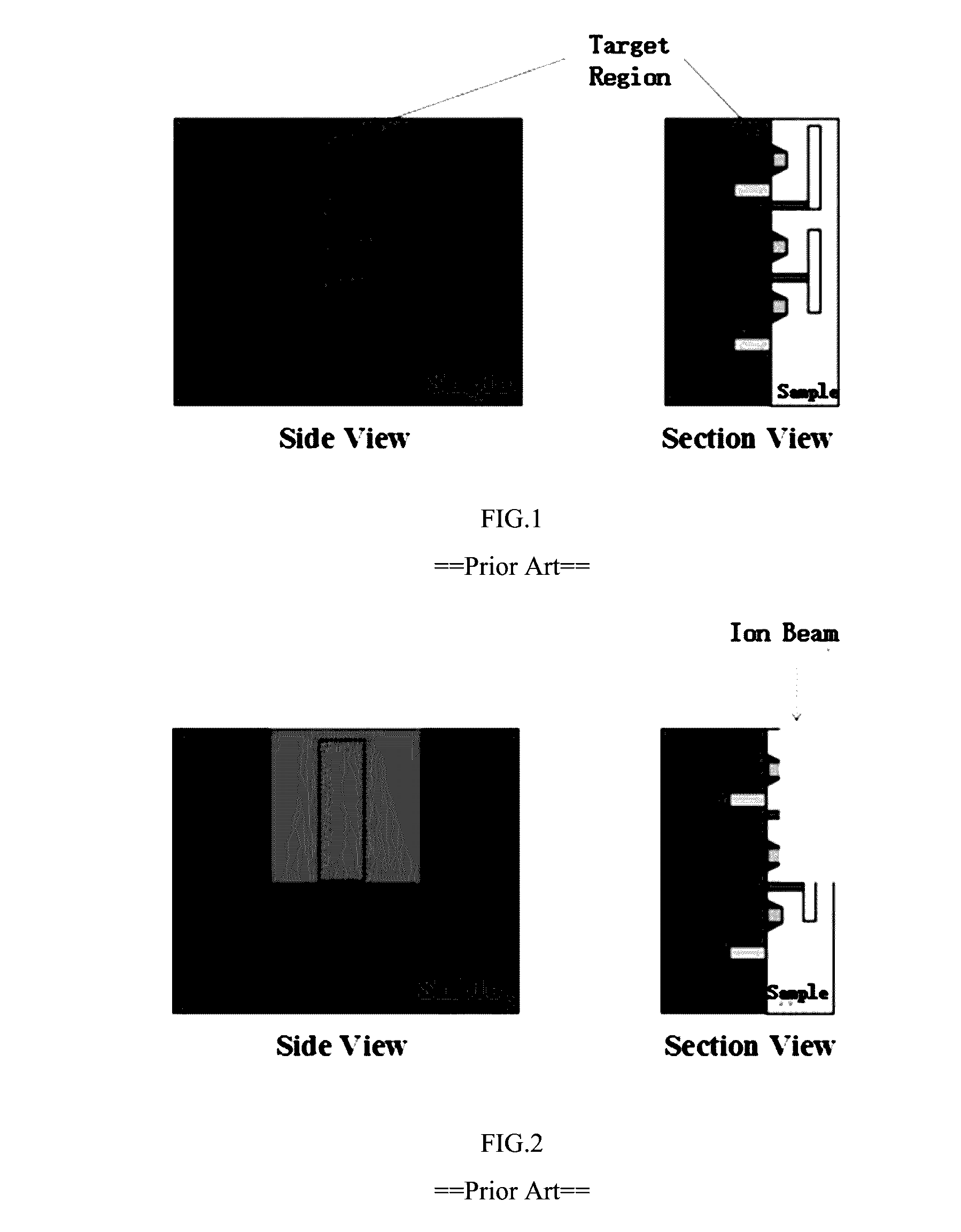
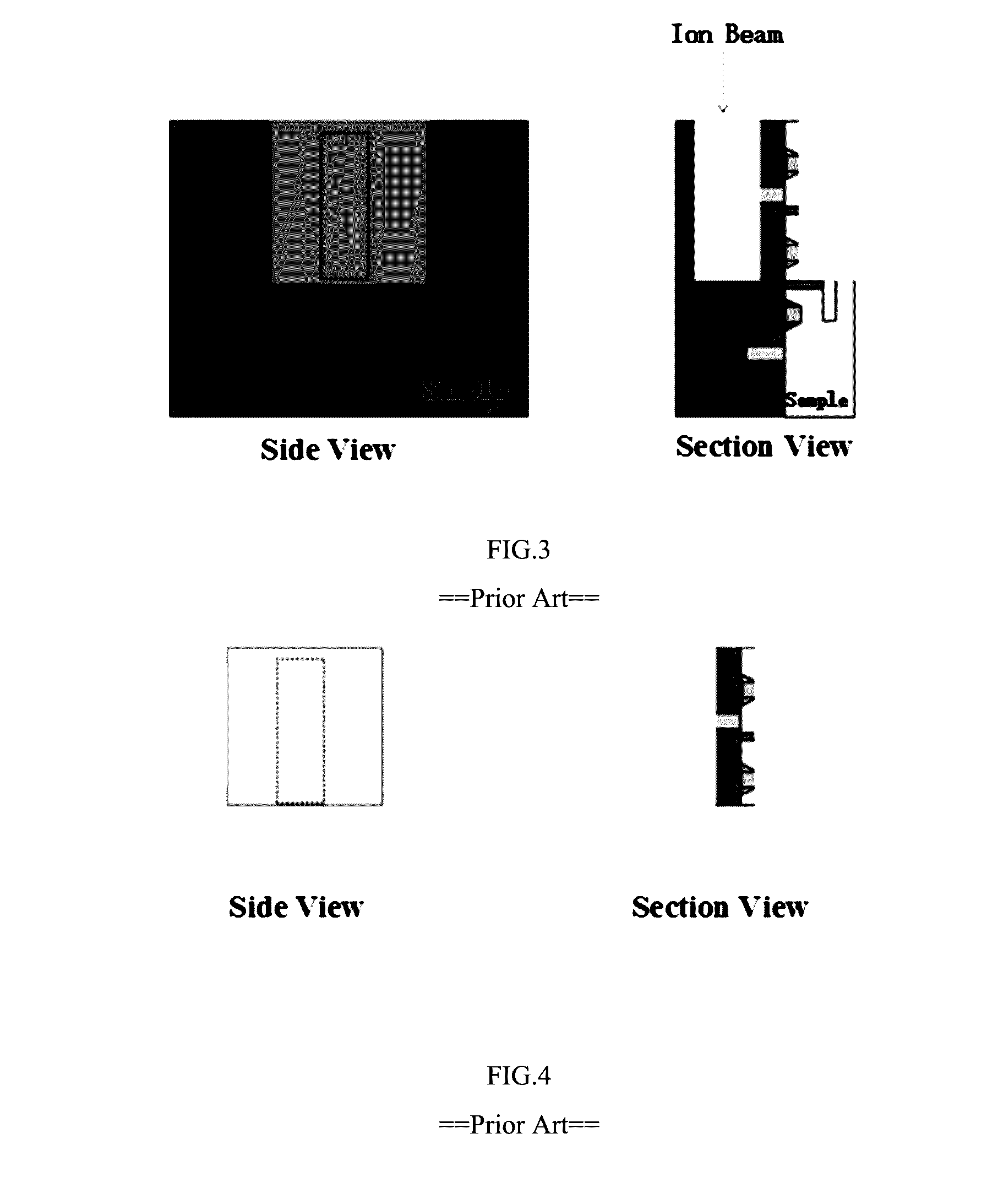
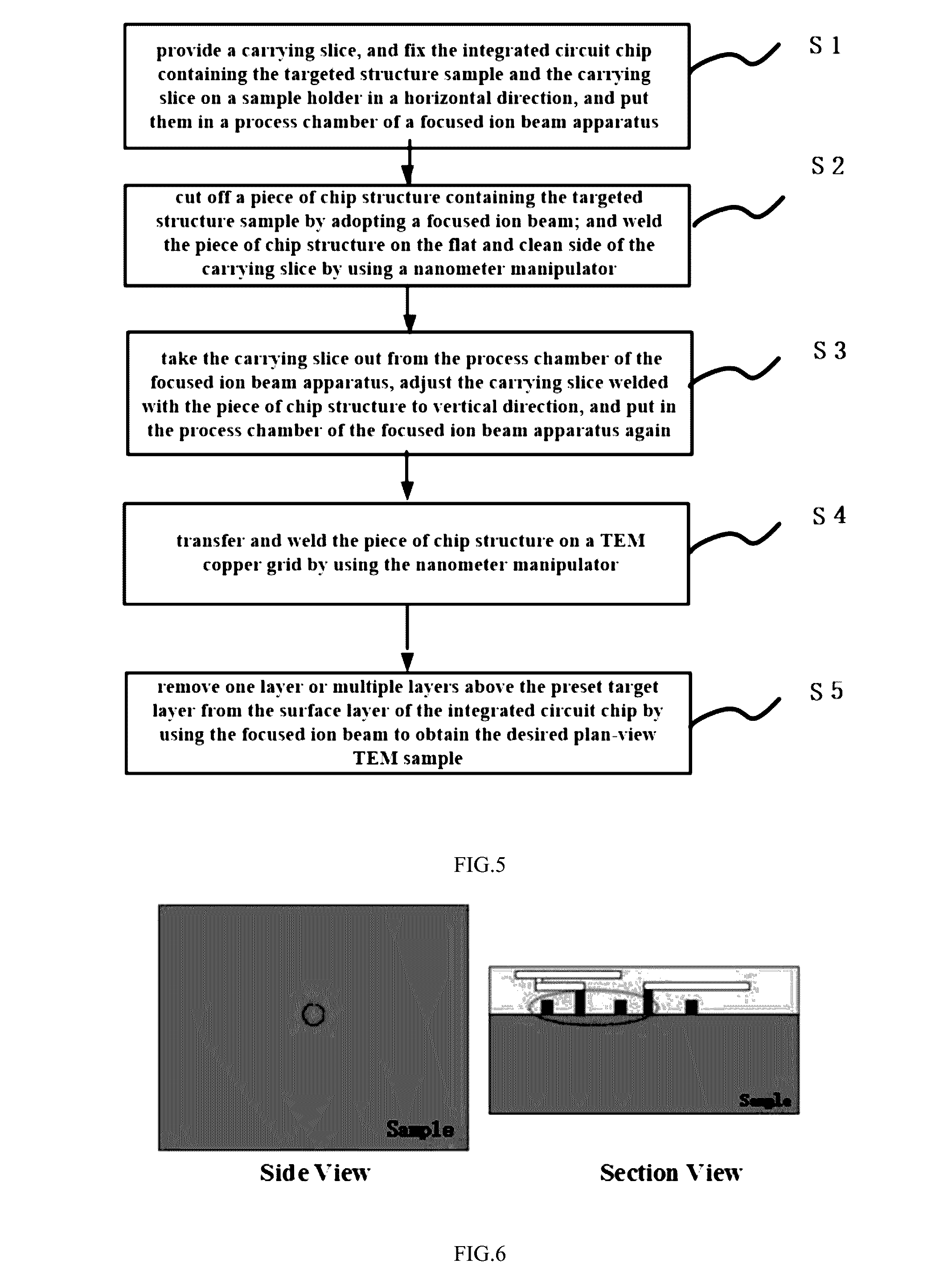
[0038]The specific embodiments of the present invention are described in detail below in combination with FIGS. 5-20. It shall be noted that, in order to satisfy the need of the subsequent detection methods, for example, in the embodiment of the present invention, at least one of preset target regions of the integrated circuit chip with a multi-layer structure is exposed, wherein a targeted structure sample to be inspected is contained in the preset target region, and the targeted structure sample may be exposed to the surface of a preset target layer, which can be understood to expose any one or more layers among the preset target layers of the integrated circuit chip with a multi-layer structure shown in FIG. 6, the preset target layers containing the target structure sample to be inspected. The preset target layer may be a gate oxide layer, CT, metal layer or the like.

[0039]In general, the multi-layer integrated circuit chip is rectangle or square, and the number of the cross sec...


PUM


Abstract

The present invention discloses a preparation method of plan-view TEM sample used in an integrated circuit analysis. The method comprises the steps of: providing a carrying slice, and fixing a chip containing a targeted structure sample and the carrying slice on a sample holder in a horizontal direction, and putting them in a process chamber of a FIB apparatus; cutting off a piece of chip structure containing a target structure sample by adopting a FIB; and welding the piece of chip structure on the flat and clean side of the carrying slice by using a nano-manipulator; after being taken out from the process chamber of the FIB apparatus, the carrying slice welded with the chip structure is adjusted to vertical direction, and is put in the process chamber of the FIB apparatus again; transferring and welding the chip structure on the TEM copper grid by using the nano-manipulator; and removing one layer or multiple layers above the preset target layer from the surface layer of the chip by using the FIB to obtain the desired plan-view TEM sample.

Description

CROSS-REFERENCE TO RELATED APPLICATION[0001]This application claims the priority benefit of Chinese Patent Application Serial No. 201510514446.0, filed Aug. 20, 2016. All disclosure of the Chinese application is incorporated herein by reference.FIELD OF THE INVENTION[0002]The present invention generally relates to the field of integrated circuit manufacturing technology, more particularly, to a method of preparing a plan-view transmission electron microscope (TEM) sample used in an integrated circuit analysis.BACKGROUND OF THE INVENTION[0003]The development of the semiconductor integrated circuit is very rapid since it appears as a new generation electronic device. In recent twenty years, the semiconductor integrated circuit undergoes three development phases, from small scale, middle scale to large scale. At present, the semiconductor integrated circuit is developing toward to the very-large-scale integration (VLSI) phase, and the development and application thereof have become one...

Claims


Application Information

Patent Timeline
Patent Type & Authority Applications(United States)
IPC IPC(8): H01J37/302H01J37/285H01J37/305
CPCH01J37/3026H01J37/285H01J37/305G01N1/286G01N1/28H01J37/26H01J2237/31745
Inventor CHEN, QIANGSHI, YANPING
Owner SHANGHAI HUALI MICROELECTRONICS CORP
Why Eureka
Try Eureka