Semiconductor device and method for forming the same

Active Publication Date: 2017-03-02
UNITED MICROELECTRONICS CORP
View PDF8 Cites 17 Cited by
  • Summary
  • Abstract
  • Description
  • Claims
  • Application Information

AI Technical Summary

Benefits of technology

[0010]It is one salient feature of the present invention that an additional thermal oxygen treatment is performed to improve the qual

Problems solved by technology

With the development of technology and the increase of original applications for electronical products, the IC devices are becoming smaller, more delicate and more diversified.
However, due to oxidation of the

Method used


Image

  • Semiconductor device and method for forming the same
  • Semiconductor device and method for forming the same
  • Semiconductor device and method for forming the same

Examples


Example

[0014]To provide a better understanding of the presented invention, preferred embodiments will be described in detail. The preferred embodiments of the present invention are illustrated in the accompanying drawings with numbered elements.

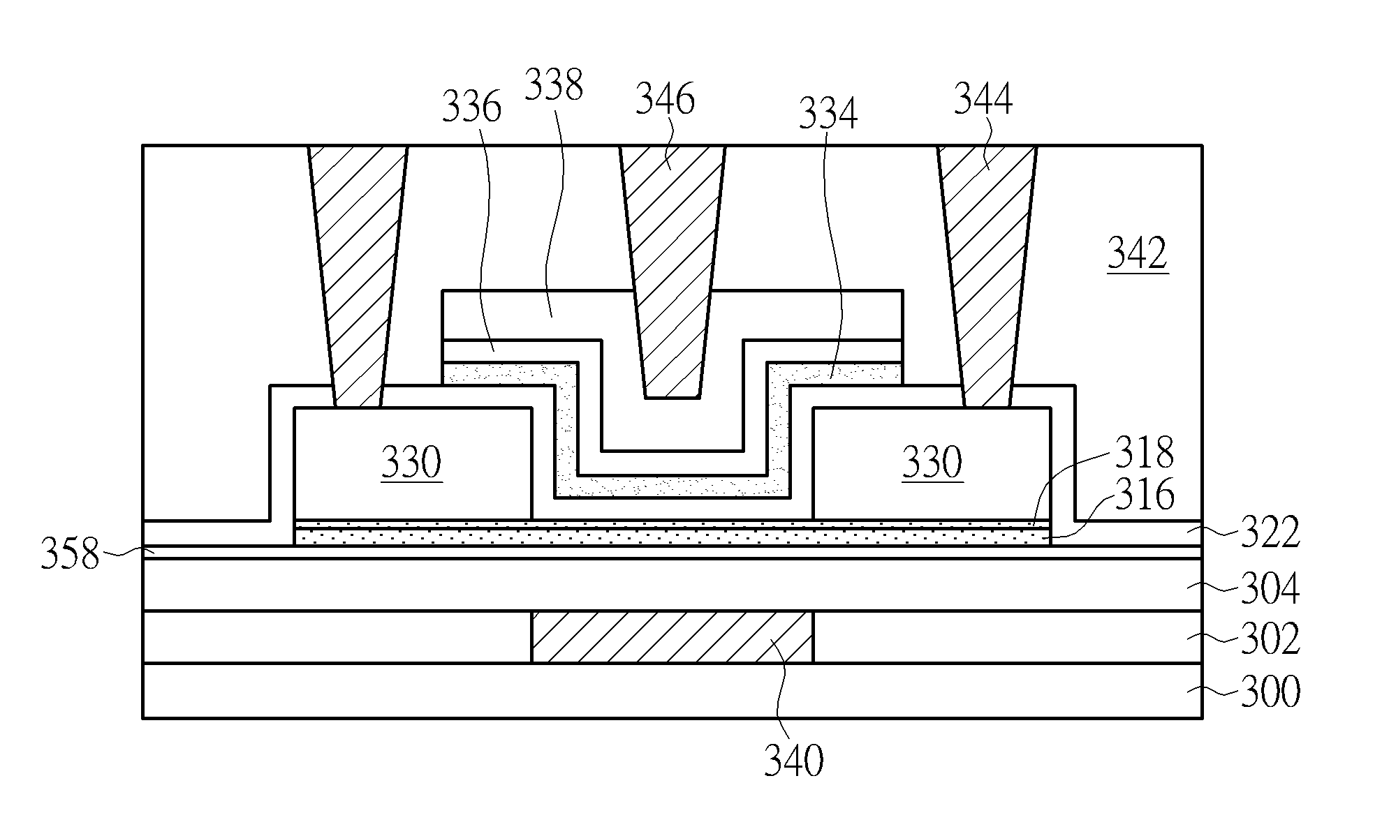
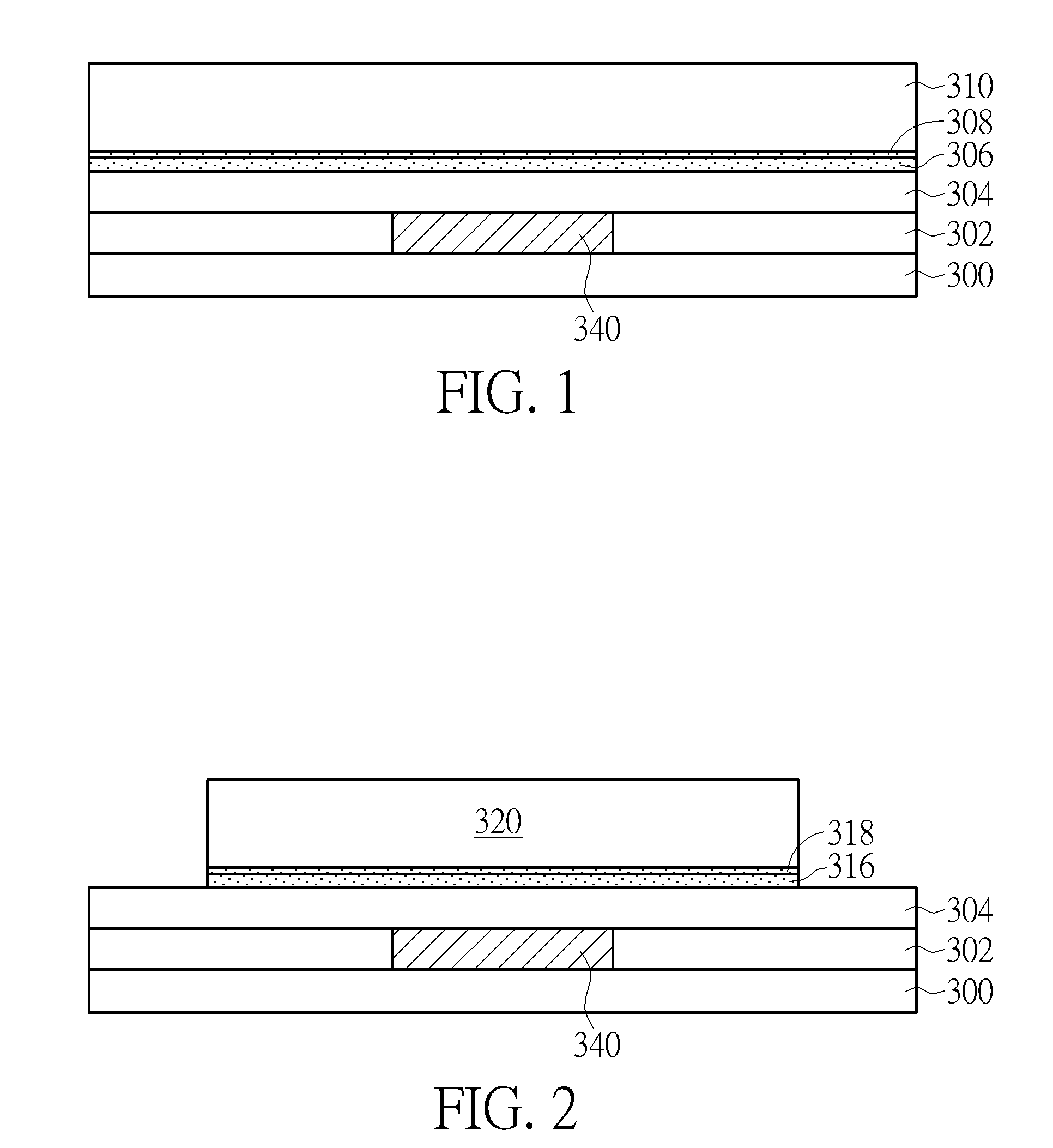
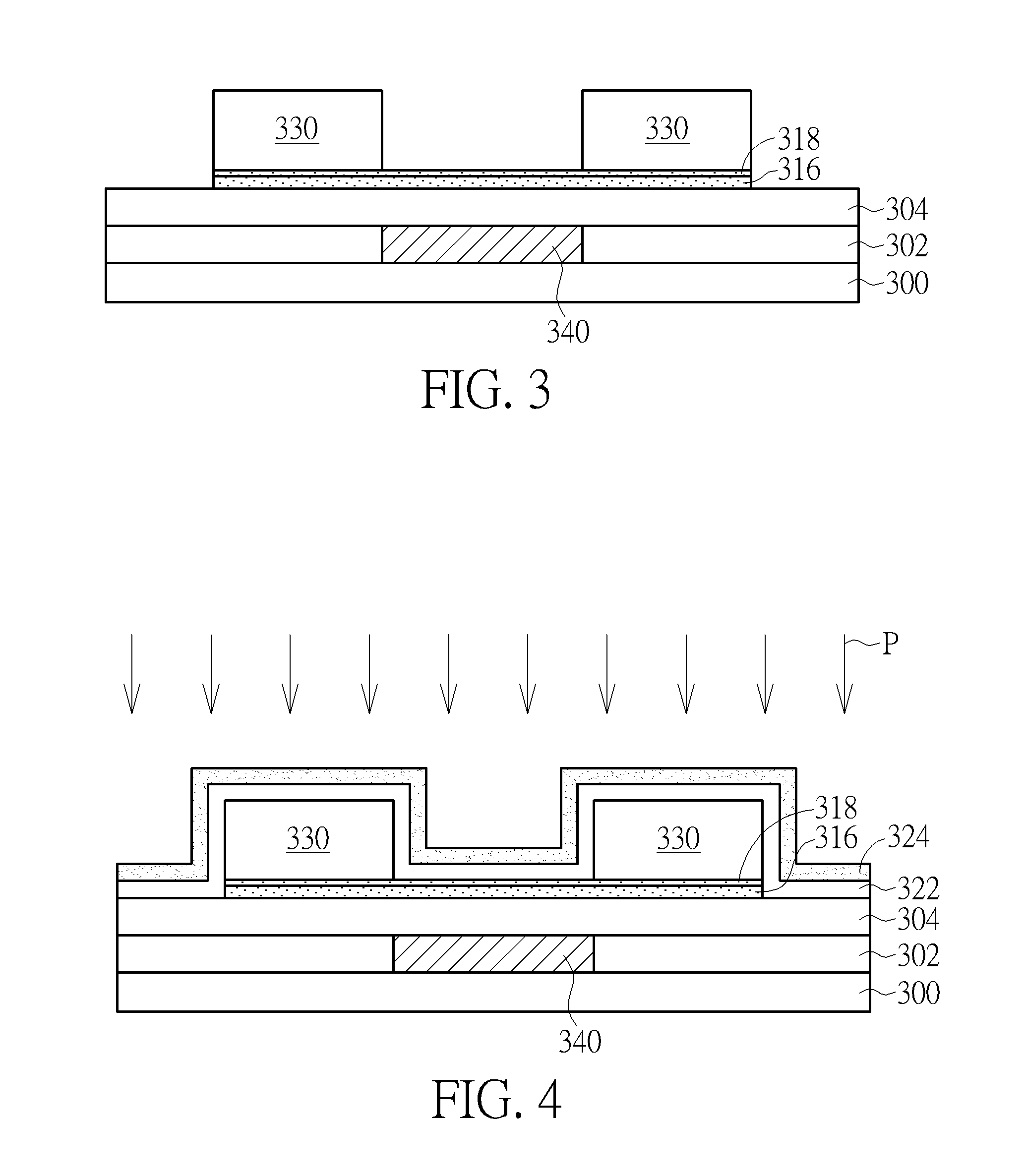
[0015]Please refer to FIG. 1 to FIG. 7, showing schematic diagrams of the method for forming a semiconductor structure according to one embodiment of the present invention. First, a substrate 300 is provided and an insulation layer 302 and an insulation layer 304 are formed sequentially on the substrate 300. The substrate 300 can be any component that can serve as a base for forming devices. In one embodiment, the substrate 300 can comprise a semiconductor material, such as a silicon substrate, an epitaxial silicon substrate, a silicon germanium substrate, a silicon carbide substrate, a single crystal silicon substrate, a single crystal silicon germanium substrate, an amorphous silicon substrate, or a silicon on insulator (SOI), but it is not limite...


PUM


Abstract

The present invention provides a semiconductor device and a method of forming the same, and the semiconductor device including a substrate, an oxide semiconductor layer, two source/drain regions, a high-k dielectric layer and a bottom oxide layer. The oxide semiconductor layer is disposed on a first insulating layer disposed on the substrate. The source/drain regions are disposed on the oxide semiconductor layer. The high-k dielectric layer covers the oxide semiconductor layer and the source structure and the drain regions. The bottom oxide layer is disposed between the high-k dielectric layer and the source/drain regions, wherein the bottom oxide layer covers the source/drain regions and the oxide semiconductor layer.

Description

BACKGROUND OF THE INVENTION[0001]1. Field of the Invention[0002]The present invention relates to a semiconductor structure and a method for forming the same, and more particularly, to a semiconductor structure having an oxide semiconductor layer and a method for forming the same.[0003]2. Description of the Prior Art[0004]In the modern society, the micro-processor systems comprising integrated circuits (IC) are ubiquitous devices, being utilized in diverse fields such as automatic control electronics, mobile communication devices and personal computers. With the development of technology and the increase of original applications for electronical products, the IC devices are becoming smaller, more delicate and more diversified.[0005]In a wide variety of materials, indium oxide (In2O3), tin oxide (SnO2) and zinc oxide (ZnO) are generally known transparent conductive oxide. Indium tin oxide is (ITO), when being formed of a thin film, can be used as a transparent electrode in a flat pane...

Claims


Application Information

Patent Timeline
IPC IPC(8): H01L27/12H01L29/51H01L29/24H01L21/768H01L29/66H01L21/02H01L21/441H01L29/786H01L23/528
CPCH01L27/1237H01L29/7869H01L29/512H01L29/24H01L23/528H01L29/66969H01L21/76897H01L27/1259H01L21/02565H01L21/02107H01L21/02323H01L21/441H01L27/1225H01L29/42384H01L29/4908H01L29/78648H01L29/78696
Inventor HSU, CHIA-FUWU, CHUN-YUAN
Owner UNITED MICROELECTRONICS CORP
Why Eureka
Try Eureka