Printed circuit board assembly having a damping layer

a technology of printed circuit boards and damping layers, which is applied in the direction of printed element electric connection formation, fixed capacitor details, and non-printed electrical components association of printed circuits, etc. it can solve the problems of pcb vibration, exacerbate the radiation of acoustic noise from the pcb, and affect the vibration of the pcb. , to achieve the effect of reducing noise radiation, reducing stiffness, and altering the vibrational characteristics of the p

Active Publication Date: 2017-03-02
APPLE INC
View PDF8 Cites 12 Cited by
  • Summary
  • Abstract
  • Description
  • Claims
  • Application Information

AI Technical Summary

Benefits of technology

[0014]A method of fabricating a PCB assembly is provided. In an embodiment, the method includes mounting several electronic components on a printed circuit board (PCB) and depositing a damping layer over the electronic components. The damping layer may be a continuous layer covering the electronic components, and may fill a lateral space between the components and be attached to the PCB. Accordingly, the damping layer may alter the vibrational characteristics of the PCB and reduce noise radiation from the PCB assembly. The method may also include depositing an overmold layer over the damping layer such that the overmold layer is attached to the PCB at several locations around the damping layer to constrain the damping layer against the PCB. Furthermore, the method may include depositing an encapsulation layer over at least one of the electronic components, e.g., a capacitor. As described above, several electronic components may be encapsulated by respective encapsulation layers such that the damping layer fills a lateral space between the encapsulated electronic components.
[0015]In an embodiment, mounting of the capacitor on the PCB includes mounting the capacitor on an interposer such that an upper contact of the interposer is electrically connected to the capacitor. The interposer may also be mounted on the PCB, such that a lower contact of the interposer is electrically connected to the PCB. Furthermore, the upper contact and the lower contact of the interposer may be electrically connected by a via having one or more via segments between different layers of the interposer. Accordingly, at least one of the via segments may be laterally offset from one or more of the upper contact or the lower contact to reduce the stiffness beneath the terminals of the capacitor, and accordingly, to reduce the transmission of excitatory vibrations from the capacitor to the PCB.
[0016]In an embodiment, an epoxy-coated capacitor is provided. The epoxy-coated capacitor may be mounted on a PCB and / or may be incorporated in a PCB assembly. For example, the epoxy-coated capacitor may be mounted directly on the PCB or it may be mounted on an interposer that is electrically connected to the PCB. In an embodiment, the capacitor includes a capacitor body having a top surface and a periphery. The periphery may include a first height, and a coating may cover the top surface and a portion of the periphery. For example, the coating may include an epoxy that covers a portion of the periphery having a second height that is less than the first height. By way of example, the second height may be between 0.8 and 0.99 of the first height. In an embodiment, the epoxy is a low modulus epoxy. For example, the epoxy may include a modulus less than 1.0 GPa and / or less than 0.5 GPa, e.g., between 0.2 and 0.5 GPa. Accordingly, the low modulus epoxy coating may dampen excitatory vibrations from the capacitor.

Problems solved by technology

Furthermore, the deformation of the electronic components can transmit deforming loads to the PCB, which can cause the PCB to vibrate.
Such vibration may lead to radiation of audible acoustic noise from the PCB and the electronic devices of the PCB assembly.
The waterproofing layer, however, is typically over-molded using a rigid epoxy, so although it may prevent ingress of moisture to the electronic components, it can actually exacerbate the radiation of acoustic noise from the PCB assembly.
More particularly, the electronic components can force the rigid waterproofing layer to vibrate along with the PCB, which may lead to increased acoustic noise radiation.
This increased acoustic noise from the PCB assembly may be undesirable for a user of an electronic device that includes the waterproofed PCB assembly.

Method used


Image

  • Printed circuit board assembly having a damping layer
  • Printed circuit board assembly having a damping layer
  • Printed circuit board assembly having a damping layer

Examples


Embodiment Construction

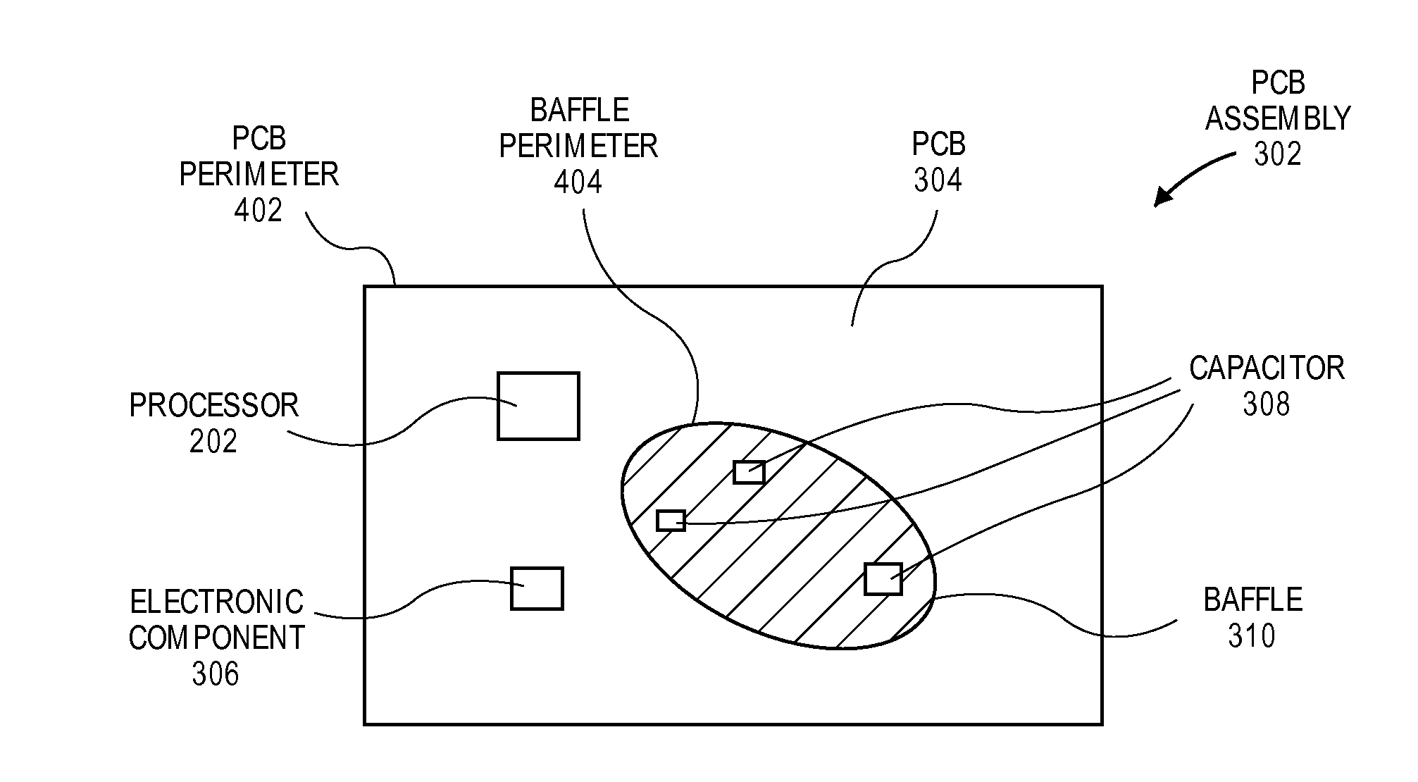
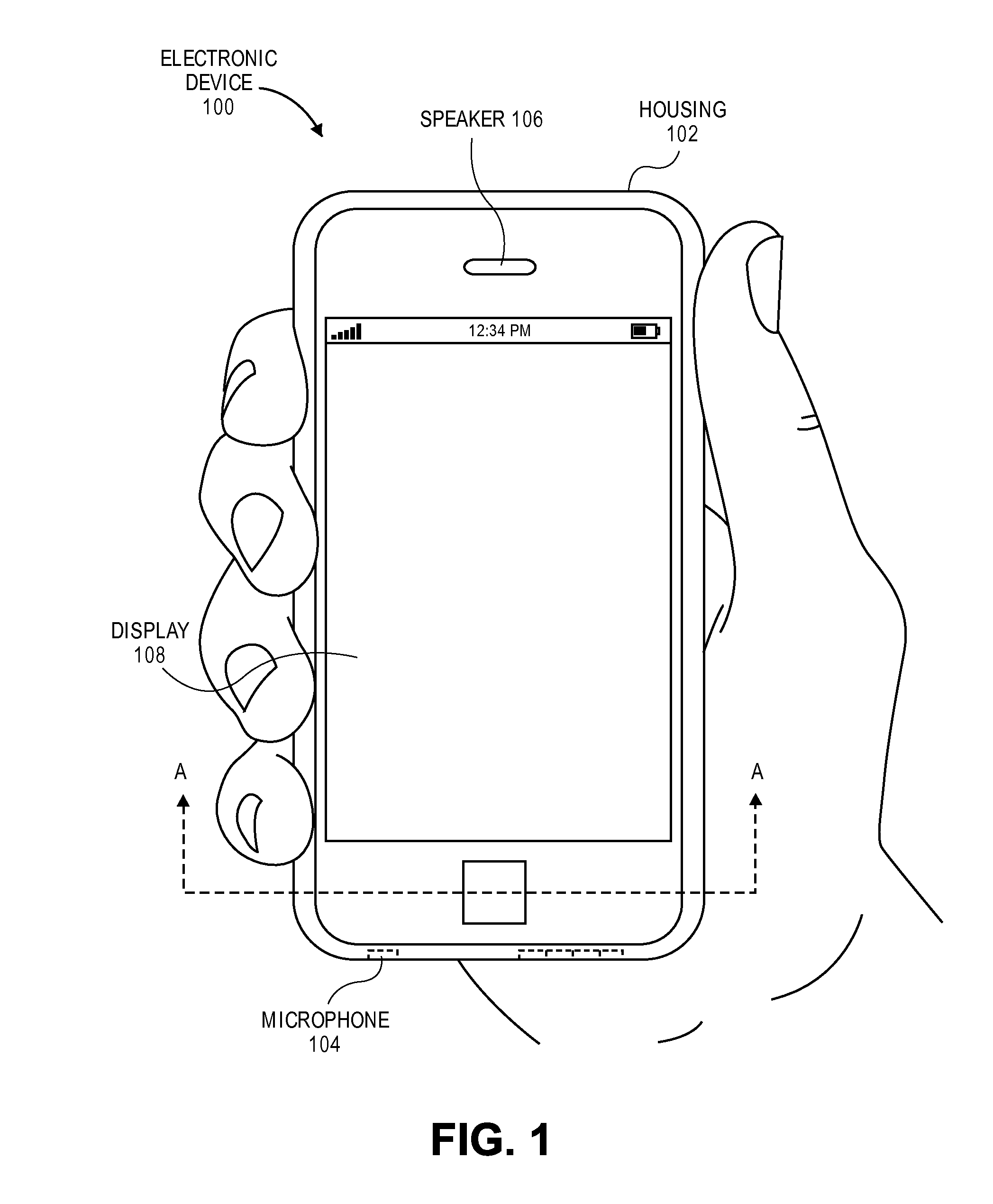
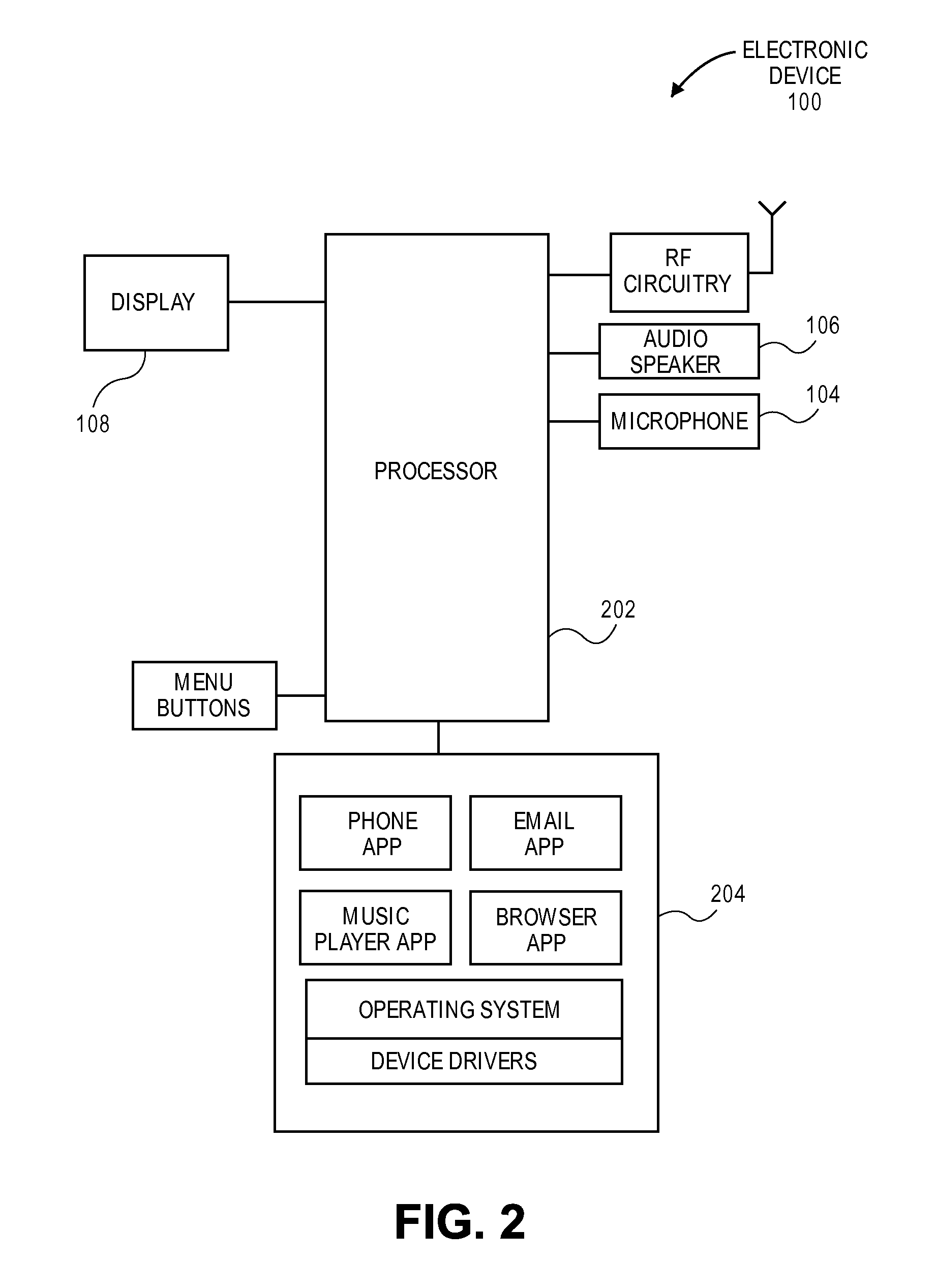
[0036]Embodiments describe printed circuit board (PCB) assemblies having one or more mechanisms to waterproof electronic components without substantially increasing acoustic noise radiation from the PCB assembly, particularly for use in electronic device applications. Some embodiments are described with specific regard to integration within mobile devices such as mobile phones. The embodiments are not so limited, however, and certain embodiments may also be applicable to other uses. For example, a PCB assembly as described below may be incorporated into other devices and apparatuses, including desktop computers, laptop computers, or motor vehicles, to name only a few possible applications.

[0037]In various embodiments, description is made with reference to the figures. Certain embodiments, however, may be practiced without one or more of these specific details, or in combination with other known methods and configurations. In the following description, numerous specific details are s...


PUM


Abstract

A printed circuit board (PCB) assembly having several electronic components mounted on a PCB and a damping layer covering the electronic components, is disclosed. Embodiments of the PCB assembly include an overmold layer constraining the damping layer against the PCB. Embodiments of the PCB assembly include an interposer between a capacitor of the electronic components and the PCB. Other embodiments are also described and claimed.

Description

BACKGROUND[0001]Field[0002]Embodiments related to printed circuit board (PCB) assemblies are disclosed. More particularly, embodiments related to PCB assemblies having several electronic components mounted on a PCB are disclosed.[0003]Background Information[0004]An electronic device, such as a computer and / or a mobile device, may include a printed circuit board (PCB) assembly having electronic components, such as integrated circuits and capacitors, mounted on a PCB. The electronic components may be electrically connected through a printed circuit having vias and traces. The electronic components may deform when a voltage ripple occurs in a driving electrical signal delivered through the printed circuit. Furthermore, the deformation of the electronic components can transmit deforming loads to the PCB, which can cause the PCB to vibrate. Such vibration may lead to radiation of audible acoustic noise from the PCB and the electronic devices of the PCB assembly.SUMMARY[0005]A printed cir...

Claims


Application Information

Patent Timeline
Patent Type & Authority Applications(United States)
IPC IPC(8): H05K1/02H05K1/11H01G4/30H05K3/40H01G4/224H05K1/18H05K3/30
CPCH05K1/0213H05K1/181H05K1/0298H05K1/115H05K2201/10015H05K3/4038H01G4/224H01G4/30H05K3/301H05K1/0271H05K1/18H05K2201/04H05K2201/10227H05K2201/2045H01G2/06H05K1/141H05K3/284H05K2201/049H05K2203/1316H05K2203/1322
Inventor LI, GEMINMARTINEZ, PAULBARD, BENJAMIN A.DUKE, CONNOR R.GONG, ZHONG-QINGRICHARDSON, KEVIN R.MEAD, CURTIS C.POULAIN, KIERANYOO, SUNG WOOKOTTKE, NELSON J.
Owner APPLE INC
Why Eureka
Try Eureka