Integrated circuits (ICS) on a glass substrate

Active Publication Date: 2017-03-23
QUALCOMM INC
View PDF0 Cites 22 Cited by
  • Summary
  • Abstract
  • Description
  • Claims
  • Application Information

AI Technical Summary

Benefits of technology

[0007]One particular advantage provided by at least one of the disclosed aspects, examples, and/or implementations is that physical and electrical separation of the first semiconductive region and the second semiconductive region may enable superior electrical isolation between the first semiconductor device and the second semiconductor device as compared to semiconductor devices that include channel regions formed

Problems solved by technology

During operation of the RF ICs, electric fields from high-frequency signals (e.g., RF signals) may diffuse into the silicon substrate layer of the bulk silicon wafer or the SOI wafer, resulting in signal leakage and inducing electrical non-linearity (e.g., edd

Method used


Image

  • Integrated circuits (ICS) on a glass substrate
  • Integrated circuits (ICS) on a glass substrate
  • Integrated circuits (ICS) on a glass substrate

Examples


Embodiment Construction

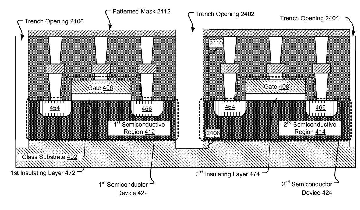
[0039]FIG. 1 illustrates an example of an integrated circuit (IC) (or a portion of an IC) 100 that includes a first semiconductor device 122 and a second semiconductor device 124 formed using a silicon-on-insulator (SOI) wafer and disposed on a glass substrate 102. The first semiconductor device 122 may be adjacent to the second semiconductor device 124 (e.g., the first and second semiconductor devices 122 and 124 may be neighbor devices). In some examples, the first semiconductor device 122 and the second semiconductor device 124 may correspond to a complementary pair of metal-oxide semiconductor field effect transistors (MOSFETS) of a complementary metal oxide semiconductor (CMOS) device. In some examples, the IC 100 may be configured to operate in a radio frequency (RF) application, e.g., as a portion of an RF component. For example, the IC 100 may be configured to operate as an RF switch. In this example, the IC 100 may include or be coupled to one or more passive devices (e.g.,...


PUM


Abstract

An integrated circuit (IC) includes a first semiconductor device on a glass substrate. The first semiconductor device includes a first semiconductive region of a bulk silicon wafer. The IC includes a second semiconductor device on the glass substrate. The second semiconductor device includes a second semiconductive region of the bulk silicon wafer. The IC includes a through substrate trench between the first semiconductive region and the second semiconductive region. The through substrate trench includes a portion disposed beyond a surface of the bulk silicon wafer.

Description

I. FIELD[0001]The present disclosure is generally related to integrated circuits including glass substrates.II. DESCRIPTION OF RELATED ART[0002]Advances in technology have resulted in smaller and more powerful computing devices. For example, a variety of portable personal computing devices, including wireless telephones, such as mobile and smart phones, tablets and laptop computers, are small, lightweight, and easily carried by users. Many such devices incorporate functionality, such as a digital still camera, a digital video camera, a digital recorder, and an audio file player. Also, such devices can process executable instructions, including software applications, such as a web browser application, that can be used to access the Internet. As such, these devices can include significant computing capabilities.[0003]These devices may also communicate voice and data packets over wireless networks using radio frequency (RF) transmissions. Accordingly, these devices may include integrat...

Claims


Application Information

Patent Timeline
IPC IPC(8): H01L23/498H01L21/8234H01L21/306H01L27/088H01L27/12H01L23/66H01L21/84H01L21/304
CPCH01L23/49894H01L21/84H01L21/823481H01L21/30604H01L27/088H01L27/1203H01L23/66H01L21/304H01L29/66772H01L27/1222H01L27/1248H01L27/1255H01L27/1266H01L21/76251H01L21/76802H01L21/76877H01L21/76895H01L27/1207H01L23/528H01L27/092H01L29/1087
Inventor GU, SHIQUNKIM, DAEIK DANIELNOWAK, MATTHEW MICHAELKIM, JONGHAEYUN, CHANGHAN HOBIELAN, JE-HSIUNG JEFFREYBERDY, DAVID FRANCIS
Owner QUALCOMM INC
Why Eureka
Try Eureka