Semiconductor photosensitive unit and semiconductor photosensitive unit array thereof

Active Publication Date: 2017-03-23
SUZHOU ORIENTAL SEMICONDUCTOR CO LTD
View PDF1 Cites 47 Cited by
  • Summary
  • Abstract
  • Description
  • Claims
  • Application Information

AI Technical Summary

Benefits of technology

[0026]The present invention has significant advantages as compared with the prior art in that:
[0027]1. during light sensing of the semiconductor photosensitive unit of the present invention, the gating MOS transistor is switched on, the floating gate of the floating gate transistor is charged using the photodiode, and when charges are stored in the floating gate of the floating gate transistor, the gating MOS transistor is switched off, such that the floating gate is prevented from leaking charges and the charge storage time of the floating gate is incre

Problems solved by technology

The charge-coupled device image sensors have advantages such as high image quality and low noise, but have high production cost and are difficult to be integrated with a peripheral circuit.
The defect of the CMOS image sensor is that, the four independently working MOS transistors occupy a large substrate area in the single pixel unit of the CMOS image sensor, the product pixel is low, and the product resolution is not high.
However, to guarantee the performance of the semiconductor photosensitive device, the planar-channel semiconductor photosensitive device also requires a long current channel, which increases the area of the semiconductor photosensitive devic

Method used


Image

  • Semiconductor photosensitive unit and semiconductor photosensitive unit array thereof
  • Semiconductor photosensitive unit and semiconductor photosensitive unit array thereof
  • Semiconductor photosensitive unit and semiconductor photosensitive unit array thereof

Examples


first embodiment

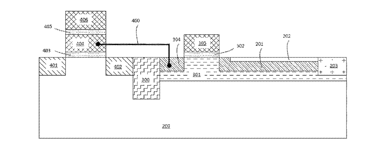
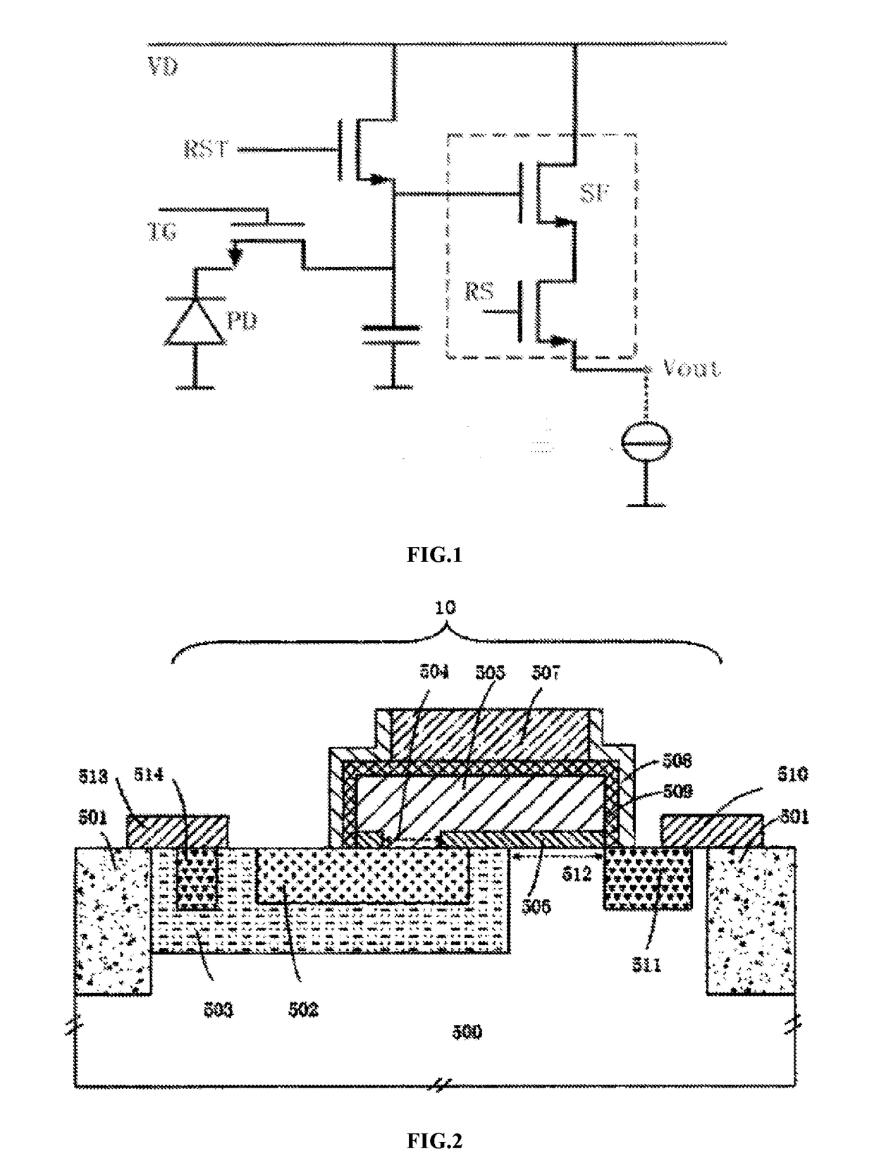
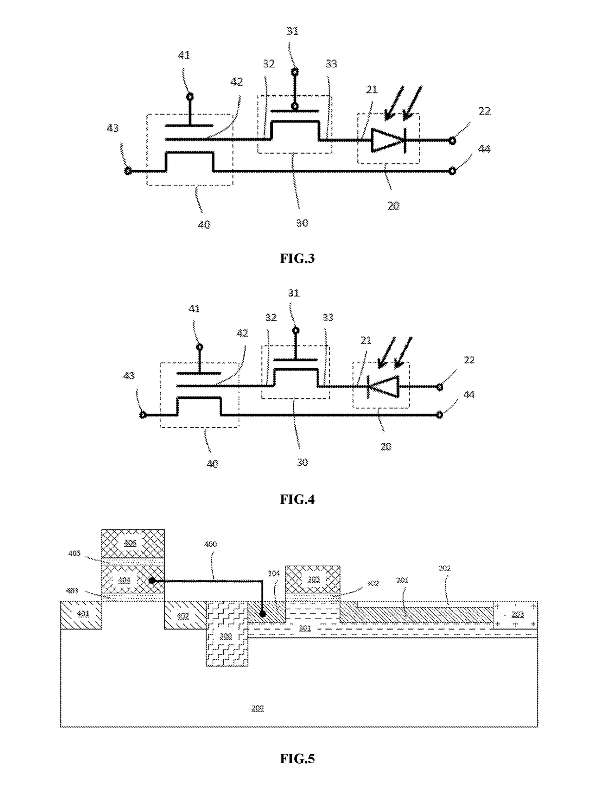
[0040]FIG. 5 is a cross-sectional diagram of the semiconductor photosensitive unit in the present invention as illustrated by the equivalent circuits in FIG. 3 and FIG. 4. As shown in FIG. 5, the semiconductor photosensitive unit of the present invention includes a doped well 301 of the second conductivity type formed in a semiconductor substrate 200 of the first conductivity type, and the semiconductor substrate 200 includes, but is not limited to, a silicon substrate, a germanium substrate, a silicon germanium substrate, or a silicon-on-insulator substrate; a diffusion region 304 and a photosensitive region 201 of the first conductivity type are disposed in the doped well 301 of the second conductivity type, a second current channel region is formed in the part of the semiconductor substrate between the diffusion region 304 and the photosensitive region 201 of the first conductivity type, and a third-layer insulation film 302 and a second control gate 303 are sequentially disposed...

second embodiment

[0049]FIG. 6 is a cross-sectional diagram of the semiconductor photosensitive unit in the present invention provided based on the two equivalent circuits of the semiconductor photosensitive unit in the present invention illustrated in FIG. 3 and FIG. 4. The semiconductor photosensitive unit illustrated in FIG. 6 is an improvement to the structure of the semiconductor photosensitive unit illustrated in FIG. 5. In the semiconductor photosensitive unit illustrated in FIG. 5, the floating gate 404 is electrically connected to the diffusion region 304 of the first conductivity type by the electrical connection line 400, while in the semiconductor photosensitive unit illustrated in FIG. 6, the floating gate 404 of the first conductivity type directly extends onto the diffusion region 304 of the first conductivity type and contacts the diffusion region 304 of the first conductivity type, such that the floating gate 404 of the first conductivity type is directly connected to the diffusion r...

third embodiment

[0050]FIG. 7 is a three-dimensional structural diagram of the semiconductor photosensitive unit in the present invention provided based on the two equivalent circuits of the semiconductor photosensitive unit in the present invention illustrated in FIG. 3 and FIG. 4. The semiconductor photosensitive unit illustrated in FIG. 7 is an improvement to the structure of the semiconductor photosensitive unit illustrated in FIG. 6. In the semiconductor photosensitive unit illustrated in FIG. 6, the first current channel region and the second current channel region are of a parallel structure; while in the semiconductor photosensitive unit illustrated in FIG. 7, the first current channel region and the second current channel region are of a vertical structure. Compared with the semiconductor photosensitive unit illustrated in FIG. 6, it is easier to control the manufacturing process of the semiconductor photosensitive unit illustrated in FIG. 7.

[0051]FIG. 8 and FIG. 9 are two equivalent circui...


PUM


Abstract

The present invention relates to a semiconductor photosensitive unit and a semiconductor photosensitive unit array thereof, including a floating gate transistor, a gating MOS transistor and a photodiode that are disposed on a semiconductor substrate. An anode or a cathode of the photodiode is connected to a floating gate of the floating gate transistor through the gating MOS transistor, and the corresponding cathode or anode of the photodiode is connected to a drain of the floating gate transistor or connected to an external electrode. After the gating MOS transistor is switched on, the floating gate is charged or discharged through the photodiode; and after the gating MOS transistor is switched off, charges are stored in the floating gate of the floating gate transistor. Advantages like a small unit area, low surface noise, long charge storage time of the floating gate, and large dynamic range of an operating voltage are achieved.

Description

BACKGROUND OF THE INVENTION[0001]Field of the Invention[0002]The present invention relates to a CMOS image sensor, and more particularly to a semiconductor photosensitive unit and a semiconductor photosensitive unit array thereof.[0003]Description of Related Art[0004]The existing image sensors are mainly divided into two types: charge-coupled device image sensors and CMOS image sensors. The charge-coupled device image sensors have advantages such as high image quality and low noise, but have high production cost and are difficult to be integrated with a peripheral circuit. The CMOS image sensors have high integration level, small volume, low power consumption, and a wide dynamic range, are compatible with the manufacturing process of the charge-coupled device image sensors, and meet the condition of high system integration. Therefore, the CMOS image sensors have become a research focus in recent years.[0005]FIG. 1 illustrates an existing CMOS image sensor composed of a circuit of a ...

Claims


Application Information

Patent Timeline
IPC IPC(8): H01L27/146H01L31/109H01L31/103
CPCH01L27/14614H01L31/103H01L27/14636H01L27/14643H01L31/109H01L27/14603H01L27/14616
Inventor LIU, WEILIU, LEIWANG, PENGFEI
Owner SUZHOU ORIENTAL SEMICONDUCTOR CO LTD
Why Eureka
Try Eureka