Resist sensitivity and profile improvement via acid anion control during field-guided post exposure bake

a technology of resist resin and acid anion control, which is applied in the direction of microlithography exposure apparatus, photomechanical treatment, instruments, etc., can solve the problems of resist resin latent acid image, small wavelength lithography suffers, integrated circuits have evolved into complex devices, etc., and achieve the effect of facilitating acid generation and acid generation

Active Publication Date: 2017-06-29
APPLIED MATERIALS INC
View PDF2 Cites 9 Cited by
  • Summary
  • Abstract
  • Description
  • Claims
  • Application Information

AI Technical Summary

Benefits of technology

[0011]In one embodiment, a photolithography method is provided. The method includes exposing a substrate having a photoresist layer disposed thereon to electromagnetic radiation. The photoresist layer may include a photoacid generator and the photoresist layer may be ionized. The method also includes dissociating the photoacid generator to form anions and ...

Problems solved by technology

Integrated circuits have evolved into complex devices that can include millions of components (e.g., transistors, capacitors and resistors) on a single chip.
Exposure to light may decompose the photo acid generator, which generates acid and results in a...

Method used


Image

  • Resist sensitivity and profile improvement via acid anion control during field-guided post exposure bake
  • Resist sensitivity and profile improvement via acid anion control during field-guided post exposure bake
  • Resist sensitivity and profile improvement via acid anion control during field-guided post exposure bake

Examples


Embodiment Construction

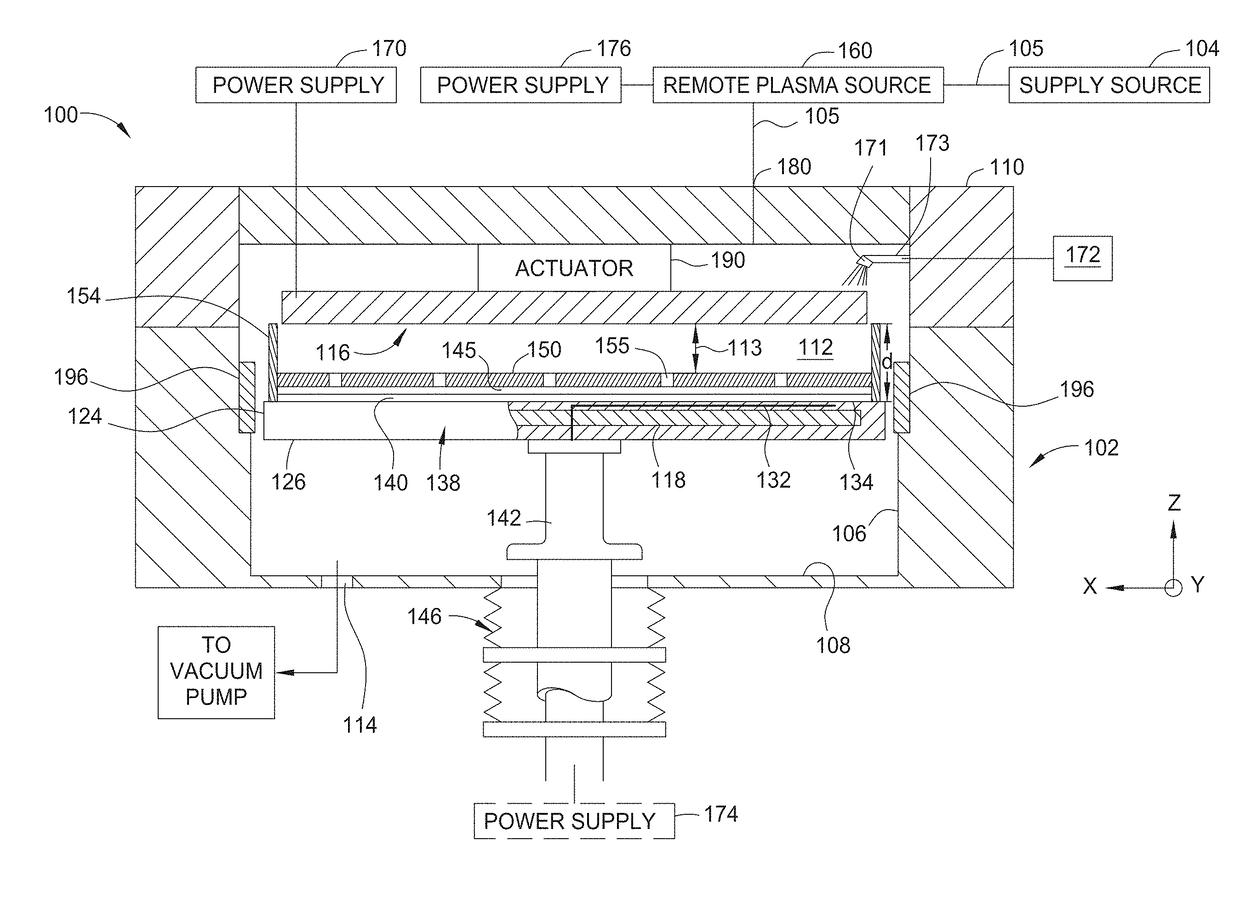
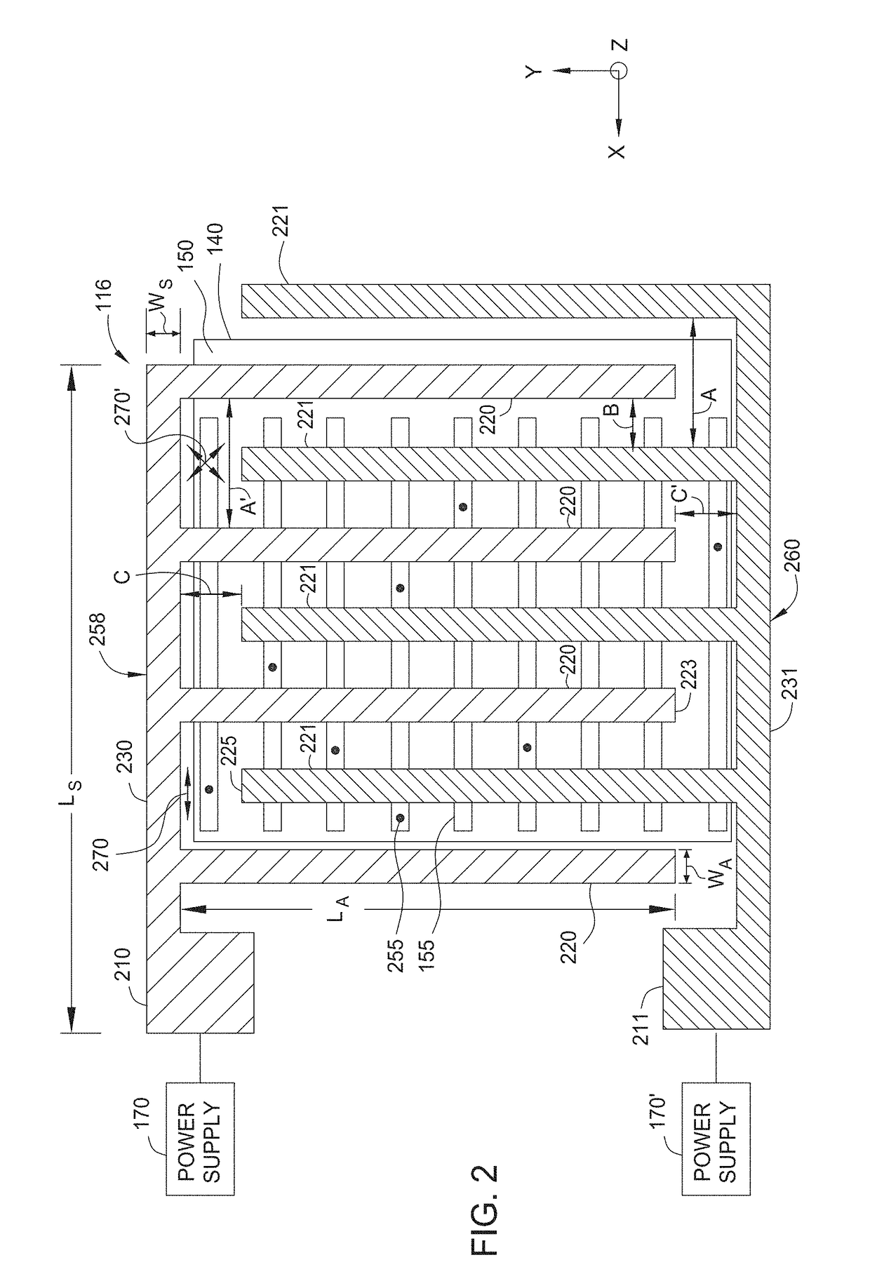
[0025]Methods and apparatus for minimizing line edge / width roughness and improving exposure resolution in a photolithography process for semiconductor applications are provided. The methods and apparatuses disclosed herein may increase the photoresist sensitivity and productivity of photolithography processes. The random diffusion of acids generated by a photoacid generator during a post-exposure bake procedure contributes to line edge / width roughness and reduced resist sensitivity. An electrode assembly may be utilized to apply an electric field and / or a magnetic field to the photoresist layer during photolithography processes. The field application may control the diffusion of the charged species generated by the photoacid generator.

[0026]An air gap defined between the photoresist layer and the electrode assembly may result in voltage drop applied to the electrode assembly, thus, adversely lowering the level of the electric field desired to be generated to the photoresist layer. A...


PUM


Abstract

Methods disclosed herein provide apparatus and methods for applying an electric field and/or a magnetic field to a photoresist layer without air gap intervention during photolithography processes. In one embodiment, an apparatus includes a processing chamber configured to apply an electric field to a substrate via a non-gas phase intermediate medium. Methods described herein include dissociation of a photoacid generator to generate anions and cations. The anions may be moved within the photoresist layer by the electric field to more precisely control the speed and location of acid generation and regeneration processes.

Description

CROSS-REFERENCE TO RELATED APPLICATIONS[0001]This application claims benefit to U.S. Provisional Patent Application No. 62 / 236,655, filed Oct. 2, 2015, the entirety of which is herein incorporated by reference.BACKGROUND[0002]Field[0003]The present disclosure generally relates to methods and apparatus for processing a substrate, and more specifically to methods and apparatus for improving photolithography processes.[0004]Description of the Related Art[0005]Integrated circuits have evolved into complex devices that can include millions of components (e.g., transistors, capacitors and resistors) on a single chip. Photolithography is a process that may be used to form components on a chip. Generally the process of photolithography involves a few basic stages. Initially, a photoresist layer is formed on a substrate. A chemically amplified photoresist may include a resist resin and a photoacid generator. The photoacid generator, upon exposure to electromagnetic radiation in the subsequen...

Claims


Application Information

Patent Timeline
IPC IPC(8): G03F7/20
CPCG03F7/70058G03F7/38G03F7/70325
Inventor OUYANG, CHRISTINE Y.NAM, SANG KIGODET, LUDOVIC
Owner APPLIED MATERIALS INC
Why Eureka
Try Eureka