Liquid crystal display device

a liquid crystal display and display device technology, applied in the direction of optical elements, polarising elements, instruments, etc., can solve the problems of defective display, reduced viewing angle characteristics, etc., to prevent the reduction of the voltage holding ratio (vhr) of liquid crystal layer, eliminate defective display generation, and increase the ion density

Active Publication Date: 2017-07-06
DAINIPPON INK & CHEM INC
View PDF1 Cites 11 Cited by
  • Summary
  • Abstract
  • Description
  • Claims
  • Application Information

AI Technical Summary

Benefits of technology

[0017]In the liquid crystal display device of the present invention, a liquid crystal composition containing a liquid crystal compound having a specific structure is used in the liquid crystal layer, and an optically anisotropic body formed through polymerization of a polymerizable liquid crystal composition that contains a polymerizable liquid crystal compound with a specific structure in the intended amount is used in the retardation layer, which prevents a reduction in the voltage holding ratio (VHR) of the liquid crystal layer and an increase in ion density (ID) and eliminates generation of defective display such as white spots, uneven alignment, and image-sticking.

Problems solved by technology

In a liquid crystal display device in which rod-like liquid crystal molecules having a positive dielectric anisotropy are used, for example, a liquid crystal cell provided with just a polarizing plate has a problem with viewing angle characteristics, in which light leaking from the liquid crystal cell is observed when it is viewed in an oblique direction.
The retardation layer containing impurities that have passed through the alignment film and the transparent electrode may cause a reduction in the voltage holding ratio (VHR) of the liquid crystal layer and defective display such as generation of white spots due to increased ion density (ID), uneven alignment, and image-sticking.
The effects of impurities remaining in the retardation layer on the liquid crystal layer, however, have not been studied.

Method used


Image

  • Liquid crystal display device
  • Liquid crystal display device
  • Liquid crystal display device

Examples


examples

[0370]Although some preferred embodiments of the present invention will now be described in detail with reference to Examples, the present invention is not limited to Examples. In compositions which will be described in Examples and Comparative Examples, the term “%” refers to “mass %”.

[0371]In Examples, the following properties were measured.

[0372]Tni: Nematic phase-isotropic liquid phase transition temperature (° C.)

[0373]Δn: Refractive index anisotropy at 25° C.

[0374]Δ∈: Dielectric anisotropy at 25° C.

[0375]η: Viscosity at 20° C. (mPa·s)

[0376]γ1: Rotational viscosity at 25° C. (mPa·s)

[0377]dgap: Gap between first and second substrates in cell (μm)

[0378]VHR: Voltage holding ratio at 70° C. (%)

[0379](ratio, represented by %, of a measured voltage to the initially applied voltage, which was obtained as follows: a liquid crystal composition was put into a cell having a thickness of 3.5 μm, and the measurement was carried out under the conditions of an applied voltage of 5 V, a frame ...

examples 1 to 4

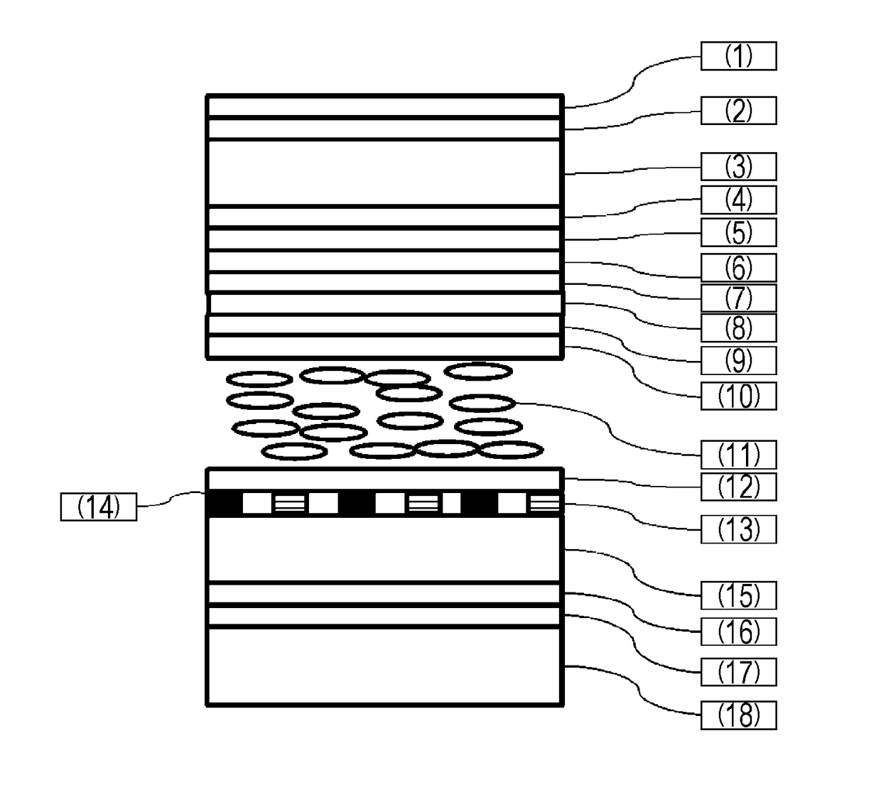
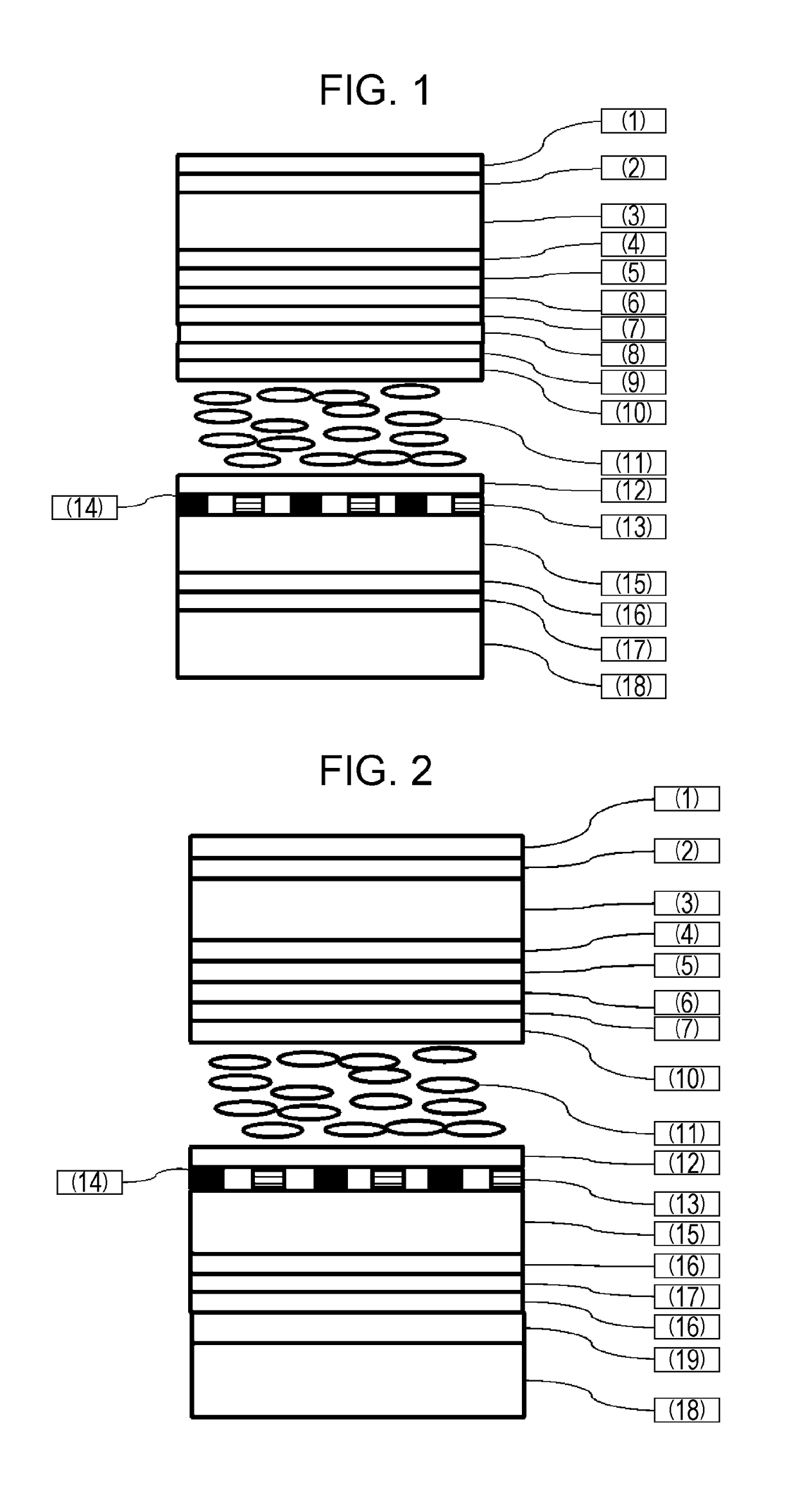
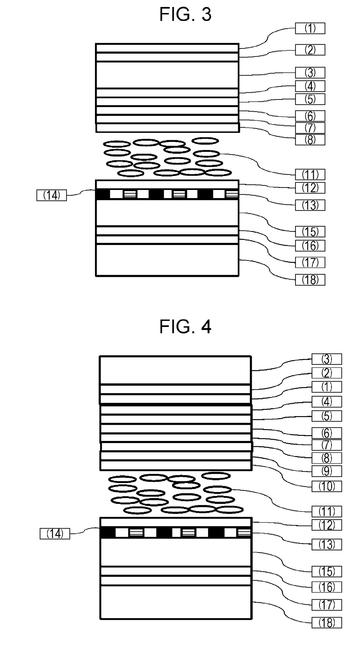
[0410]A color filter layer (4) was attached to the first light-transmitting substrate (3), and then an alignment film (6) for a retardation film was formed thereon. The polymerizable liquid crystal composition 5 was applied to the alignment film (6) for a retardation film with a spin coater, dried at 80° C. for 2 minutes, subsequently cooled at room temperature, and irradiated with 500 mJ / cm2 of ultraviolet light emitted from a high pressure mercury lamp to form a first retardation layer (7) of a positive C plate. An alignment film (8) for a retardation film was formed on the first retardation layer (7). The alignment film (8) for a retardation film was slightly rubbed, then the polymerizable liquid crystal composition 1 was applied thereto with a spin coater, dried at 80° C. for 2 minutes, subsequently cooled at room temperature, and irradiated with 500 mJ / cm2 of ultraviolet light emitted from a high pressure mercury lamp to form a second retardation layer (9) of a positive A plate...

examples 5 to 12

[0415]IPS liquid crystal display devices of Examples 5 to 12 were produced as in Example 1 except that the following liquid crystal compositions and polymerizable liquid crystal compositions were used. The VHRs and ID thereof were measured. The liquid crystal display devices were subjected to the evaluation of image-sticking. The following tables show results of the measurement and evaluation.

TABLE 6Liquid crystalLiquid crystalcomposition 2composition 3ContentContentCompounds(%)Compounds(%)4-Cy-Cy-1d0155-Cy-Cy-1d050d1-Cy-Cy-Ph-143-Cy-Cy-1d1100d3-Cy-Cy-Ph-1140d1-Cy-Cy-Ph-183-Cy-Ph-Ph-Cy-335-Cy-Cy-Ph-O163-Cy-Ph-Ph1-Cy-342-Ph-Ph1-Ph-381-Cy-Cy-Ph3-F92-Cy-Cy-Ph3-F112-Cy-Ph-Ph3-F103-Cy-Cy-Ph3-F153-Cy-Ph-Ph3-F105-Cy-Cy-Ph3-F55-Cy-Ph-Ph3-F53-Cy-Ph-Ph3-F60d1-Cy-Cy-Ph1-F83-Cy-Ph-Ph1-F93-Cy-Cy-Ph1-Ph3-F84-Cy-Cy-Ph-OCFFF42-Ph-Ph3-CFFO-Ph3-F43-Cy-Cy-CFFO-Ph3-F73-Ph-Ph3-CFFO-Ph3-F65-Cy-Cy-CFFO-Ph3-F4Tni / ° C.100.73-Cy-Cy-Ph1-Ph3-F2Δn0.094Tni / ° C.103.2Δε8.0Δn0.102γ1 / mPa · s108Δε7.1η / mPa · s22.2γ1 / m...


PUM

PropertyMeasurementUnit
thicknessaaaaaaaaaa
mass %aaaaaaaaaa
mass %aaaaaaaaaa

Abstract

The present invention provides a liquid crystal display device that is free from a reduction in the voltage holding ratio (VHR) of the liquid crystal layer and an increase in ion density (ID) and that enables problems of defective display, such as white spots, uneven alignment, and image-sticking, to be eliminated. In particular, the present invention provides a liquid crystal display device in which a liquid crystal composition containing a liquid crystal compound having a specific structure is used in the liquid crystal layer and in which an optically anisotropic body formed through polymerization of a polymerizable liquid crystal composition containing a specific amount of a polymerizable liquid crystal compound having a specific structure is used as an in-cell retardation layer.

Description

TECHNICAL FIELD[0001]The present invention relates to a liquid crystal display device.BACKGROUND ART[0002]Liquid crystal display devices have come to be applied to, for example, watches, calculators, a variety of household electrical appliances, measuring equipment, panels used in automobiles, word processors, electronic notebooks, printers, computers, and television sets. Representative examples of types of liquid crystal display devices include a TN (twisted nematic) type, an STN (super twisted nematic) type, a DS (dynamic scattering) type, a GH (guest•host) type, an IPS (in-plane switching) type, an OCB (optically compensated birefringence) type, an ECB (electrically controlled birefringence) type, a VA (vertical alignment) type, a CSH (color super homeotropic) type, and an FLC (ferroelectric liquid crystal) type. A typical drive system is static driving; however, multiplex driving has become common, and a passive matrix and, in recent years, an active matrix (AM) in which a TFT ...

Claims


Application Information

Patent Timeline
Patent Type & Authority Applications(United States)
IPC IPC(8): C09K19/38G02F1/1333C09K19/32G02F1/13363C09K19/30C09K19/34
CPCC09K19/3814G02F2001/133638C09K19/3003C09K19/3402C09K19/322G02F1/13363G02F1/133365C09K2019/0466C09K2019/3004C09K2019/3009C09K2019/301C09K2019/3016C09K2019/3019C09K2019/3021C09K2019/3422C09K2019/0448G02F2413/02G02F2413/01G02F2413/11G02F2413/13G02F2001/133633C09K19/3066C09K19/12C09K19/30C09K19/20C09K2019/122C09K2019/123C09K2019/124C09K2019/3025G02B5/3016G02F1/133565G02F1/133633C09K19/42C09K19/44G02F1/13G02B5/30G02F1/133634G02F1/133638
Inventor KURIYAMA, TAKESHIKAWAMURA, JOUJIYAMAMOTO, MIKAKUWANA, YASUHIRO
Owner DAINIPPON INK & CHEM INC
Why Eureka
Try Eureka