Electron buffering material and organic electroluminescent device
Inactive Publication Date: 2017-08-03
ROHM & HAAS ELECTRONIC MATERIALS LLC
View PDF7 Cites 4 Cited by
Summary
Abstract
Description
Claims
Application Information
AI Technical Summary
This helps you quickly interpret patents by identifying the three key elements:
Problems solved by technology
Method used
Benefits of technology
Benefits of technology
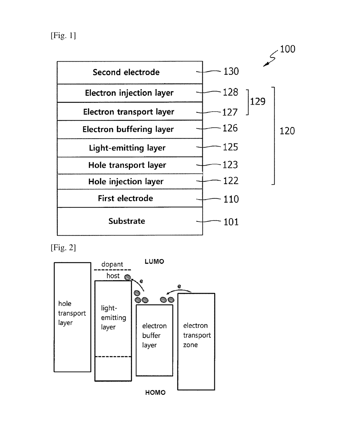
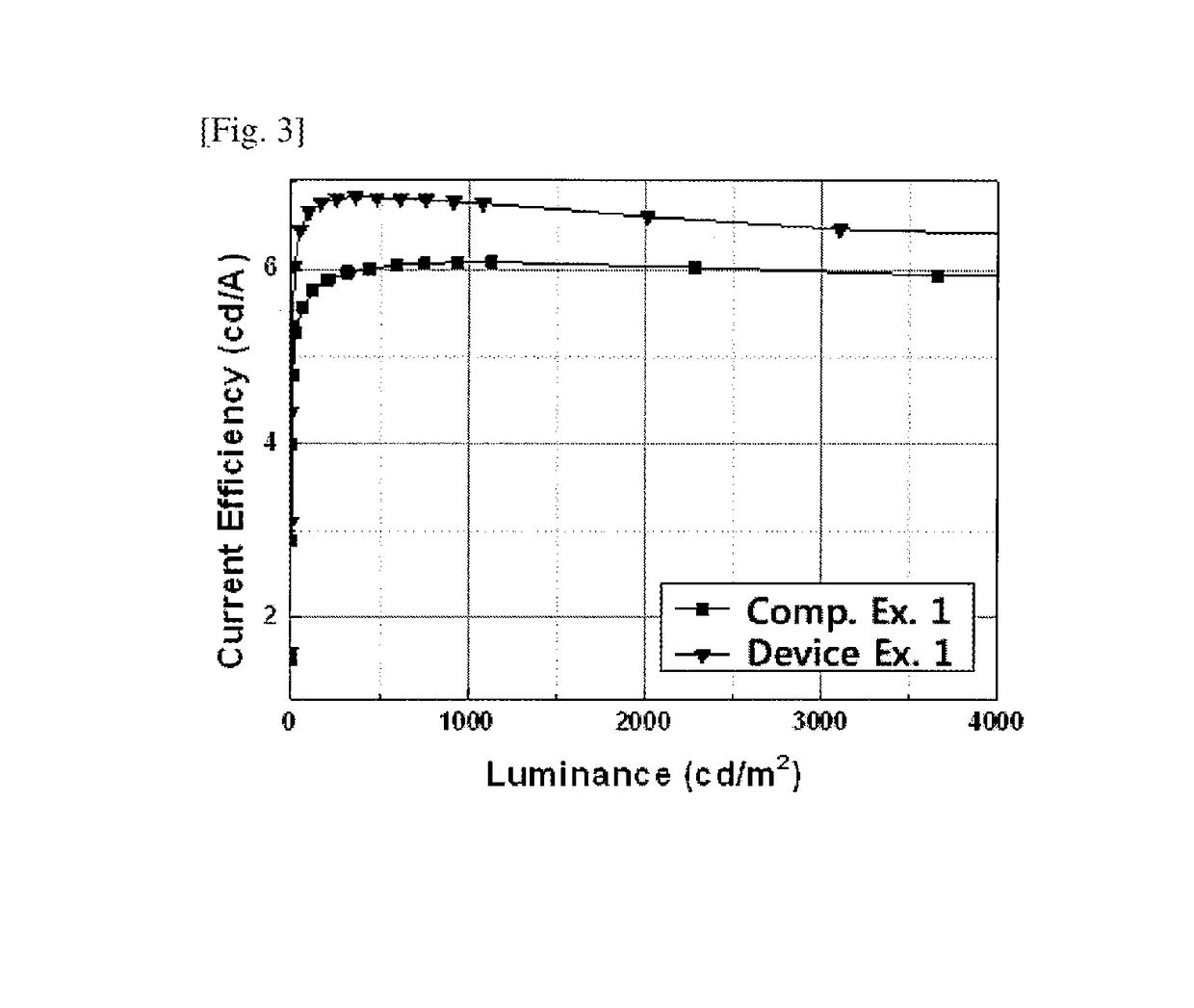
The present invention describes an electron buffering material for organic electroluminescent devices that allows for a fast electron current and efficient light emission at low driving voltage. By controlling the intermolecular 7-orbital characteristics, the electron buffering material creates a planar structure for the device, making it more effective and efficient. The patent describes a schematic sectional view and an energy band diagram of the device structure, as well as a graph showing current efficiency and luminance. Overall, the invention improves the performance of organic electroluminescent devices.
Problems solved by technology
However, in the case of blue phosphorescent materials, characteristics deteriorate due to decrease of roll-off at high current by loss of excessively formed excitons, the blue phosphorescent material itself has problems in long-term lifespan stability, and the color purity sharply drops as time passes, which are obstacles to the realization of a full color display.
First, when exposed to high temperature during a process of producing a panel, a current characteristic of the device changes to cause a problem of a change in luminance, and due to a structural characteristic, a drop of an interfacial characteristic between a light-emitting layer and an electron injection layer causes a decrease in luminance.
However, the proposed combination makes holes become greatly trapped, which can cause light-emitting sites in a light-emitting layer to shift to the side close to a hole transport layer, thereby light being emitted at an interface.
The light-emission at the interface decreases lifespan of a device, and efficiencies are not satisfactory.
It is not easy to solve the aforementioned problems of a fluorescent material by improving a light-emitting material itself.
However, the prior art reference fails to disclose an organic electroluminescent device using a compound in which a benzofuran or benzothiophene is fused to a carbazole derivative to form a backbone of the compound, in an electron buffering layer.
However, the electron buffering materials are limited to Alq3 derivatives, and have limited objectives to block electrons, and the group of compounds disclosed as buffering materials is small.
Thus, they have limitations in analyzing materials having improved luminous efficiency and lifespan.
Method used
Image
Click on the blue label to locate the original text in one second.
Reading with bidirectional positioning of images and text.
Examples
example 1
on of Compound B-3
[0059]
[0060]Preparation of Compound 1-1
[0061]After mixing 1-bromo-2-nitrobenzene (39 g, 0.19 mol), dibenzo[b,d]furan-4-yl boronic acid (45 g, 0.21 mol), Pd(PPh3)4 (11.1 g, 0.0096 mol), 2 M K2CO3 aqueous solution 290 mL, EtOH 290 mL, and toluene 580 mL, the reactant mixture was stirred for 4 hours while heated to 120° C. After the reaction is completed, the mixture was washed with distilled water, and extracted with EA. The extracted organic layer was dried with anhydrous MgSO4, and the solvent was removed with a rotary evaporator. The residue was purified by column chromatography to obtain compound 1-1 (47 g, 85%).
[0062]Preparation of Compound 1-2
[0063]After mixing compound 1-1 (47 g, 0.16 mol), triethylphosphite 600 mL, and 1,2-dichlorobenzene 300 mL, the reactant mixture was heated to 150° C. and stirred for 12 hours. After the reaction is completed, unreacted triethylphosphite and 1,2-dichlorobenzene were removed using a distillation apparatus. The remaining mix...
example 2
on of Compound B-10
[0066]
[0067]Preparation of Compound 2-1
[0068]Compound 2-1 (10 g, 32.74 mmol, 74.68%) was obtained by the synthetic method of compound 1-1 using dibenzo[b,d]thiophen-4-yl boronic acid (10 g, 43.84 mmol).
[0069]Preparation of Compound 2-2
[0070]Compound 2-2 (7 g, 25.60 mmol, 78.19%) was obtained by the synthetic method of compound 1-2 using compound 2-1 (10 g, 32.74 mmol).
[0071]Preparation of Compound B-10
[0072]The objective compound B-10 (5.6 g, 40%) was obtained by the synthetic method of compound B-3 using compound 2-2 (7 g, 25.6 mmol) and 2-chloro-4,6-diphenyl-1,3,5-triazine (8.7 g, 32.6 mmol).
example 3
on of Compound B-22
[0073]
[0074]The objective compound B-22 (5.3 g, 49%) was obtained by the synthetic method of compound B-3 using compound 2-2 (7 g, 25.6 mmol) and compound 3-1 (8.2 g, 32.6 mmol).
[0075]Compounds B-1 to B-72 were synthesized by the same method as Examples 1 to 3 above. Specific property data of the representative compounds therefrom are listed in Table 1 as below:
TABLE 1YieldMeltingUVPLMS / EIMSCompound(%)point (° C.)(nm)(nm)(found)325260358471488.5430259336463686.9626350356429581.7746225338482504.3878312344385489.5967249324458610.71040324352482505.71145255334451581.71289275320456580.71372267334459610.71546270344471593.71842288370475745.91928323N / AN / A746.82039320325516581.72138198317461504.62249274322491580.72449284368474669.825232703244567632626245300460656.82752241294464581.72842328343481656.82932294296467655.23134294N / AN / A656.83260280294468593.73446324324495589.73582250356448669.83830293344469669.83923238362429593.74044357322460655.84448278344395580.747482213343966...
PUM
Abstract
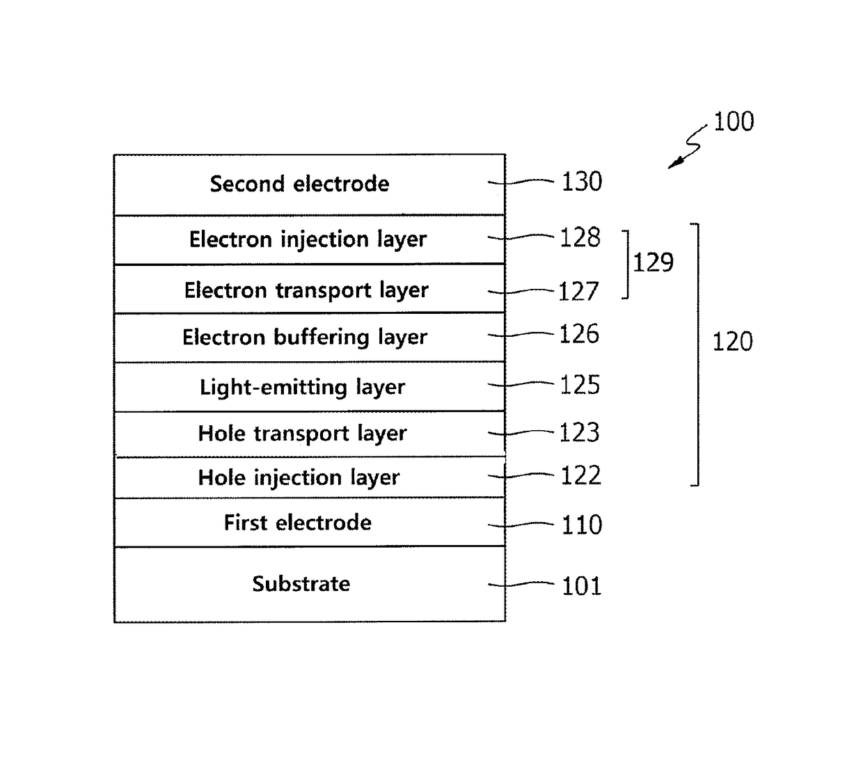
The present invention relates to an electron buffering material, and an organic electroluminescent device comprising a first electrode; a second electrode facing the first electrode; a light-emitting layer between the first electrode and the second electrode; and an electron transport zone and an electron buffering layer between the light-emitting layer and the second electrode. The electron buffering material of the present invention can produce an organic electroluminescent device having low driving voltage, excellent luminous efficiency, and long lifespan.
Description
TECHNICAL FIELD[0001]The present invention relates to an electron buffering material, and an organic electroluminescent device comprising the same.BACKGROUND ART[0002]After Tang et al. of Eastman Kodak first developed a TPD / Alq3 bilayersmall molecule green organic electroluminescent device (OLED) composed of a light-emitting layer and an charge transport layer in 1987, studies of organic electroluminescent devices have been rapidly conducted, and now became commercialized. At present, phosphorescent materials, which have excellent luminous efficiency, are mainly used for panels of the organic electroluminescent devices. In the case of red and green light-emitting organic electroluminescent devices, commercialization of organic electroluminescent devices using phosphorescent materials succeeded. However, in the case of blue phosphorescent materials, characteristics deteriorate due to decrease of roll-off at high current by loss of excessively formed excitons, the blue phosphorescent...
Claims
Application Information
Patent Timeline
Application Date:The date an application was filed.
Publication Date:The date a patent or application was officially published.
First Publication Date:The earliest publication date of a patent with the same application number.
Issue Date:Publication date of the patent grant document.
PCT Entry Date:The Entry date of PCT National Phase.
Estimated Expiry Date:The statutory expiry date of a patent right according to the Patent Law, and it is the longest term of protection that the patent right can achieve without the termination of the patent right due to other reasons(Term extension factor has been taken into account ).
Invalid Date:Actual expiry date is based on effective date or publication date of legal transaction data of invalid patent.

