Compound for organic electronic element, organic electronic element using the same, and an electronic device

a technology of organic electronic elements and organic electronic elements, applied in the direction of organic chemistry, luminescent compositions, chemistry apparatus and processes, etc., can solve the problems of longer emitting life span, achieve high luminous efficiency, prevent the interface of the emitting layer, and increase the charge balance in the emitting layer

Active Publication Date: 2017-08-24
DUK SAN NEOLUX
View PDF1 Cites 27 Cited by
  • Summary
  • Abstract
  • Description
  • Claims
  • Application Information

AI Technical Summary

Benefits of technology

[0015]By using the laminate including the emitting auxiliary layer and the hole transport layer according to the present invention, the deterioration of the interface of the emitting layer is prevented, and by increasing the charge balance in the emitting layer, thereby the high luminous efficiency, low driving voltage, high color purity, and life span can be greatly improved.

Problems solved by technology

However, it is difficult to say that organic EL element using these materials have a sufficient emitting life span, therefore, there is currently a demand for an organic EL element capable of driving at a lower voltage with higher efficiency and also having a longer emitting life span.

Method used


Image

  • Compound for organic electronic element, organic electronic element using the same, and an electronic device
  • Compound for organic electronic element, organic electronic element using the same, and an electronic device
  • Compound for organic electronic element, organic electronic element using the same, and an electronic device

Examples


synthesis example 1

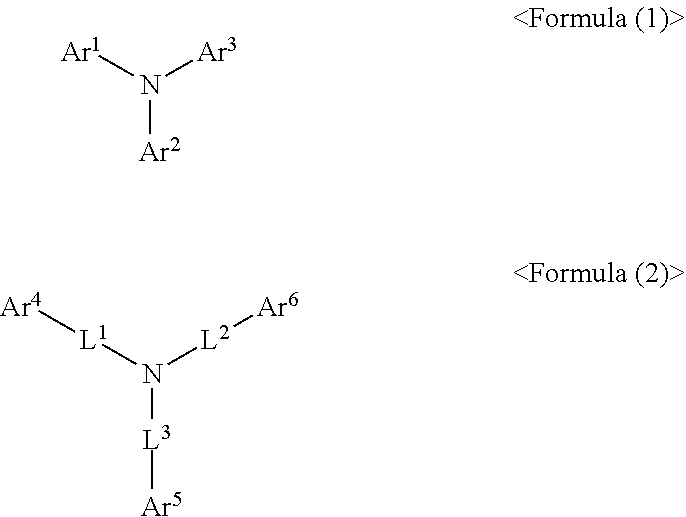
[0073]The final product 1 represented by Formula (1) according to the present invention can be synthesized by reaction between Sub 1 or Sub 2 and Sub 3 as illustrated in the following Reaction Scheme 1.

[0074]*L is L4 or L5 defined as the Formula (1-a), and the Formula (1-b).

1. Synthesis Example of Sub 1

[0075]

1) Synthesis Example of Sub 1-1-1 (L=Biphenyl)

[0076]

[0077]The starting material 9H-carbazole (50.16 g, 300 mmol) in 4-bromo-4′-iodo-1,1′-biphenyl (129.2 g, 360 mmol), Na2SO4 (42.6 g, 300 mmol), K2CO3 (41.4 g, 300 mmol), Cu (5.72 g, 90 mmol), nitrobenzene using the synthesis method Sub 1, the product 80.05 g (yield: 67%) was obtained.

2) Synthesis Examples of Sub 1-1-2 (L=9,9-Dimethyl-9H-Fluorene)

[0078]

[0079]The starting material 9H-carbazole (50.16 g, 300 mmol) in 2-bromo-7-iodo-9,9-dimethyl-9H-fluorene (143.7 g, 360 mmol), Na2SO4 (42.6 g, 300 mmol), K2CO3 (41.4 g, 300 mmol), Cu (5.72 g, 90 mmol), nitrobenzene using the synthesis method Sub 1, the product 88.11 g (yield: 67%) was...

synthesis examples

of 1-32

[0113]

[0114]After 3-(4-bromophenyl)-9-phenyl-9H-carbazole (9.6 g, 24 mmol) was dissolved in toluene, followed by being added respectively N-([1,1′-biphenyl]-4-yl)-9,9-dimethyl-9H-fluoren-2-amine (7.2 g, 20 mmol), Pd2(dba)3 (0.05 equiv), PPh3 (0.1 equiv), NaOt-Bu (3 equiv) followed by reflux and stirring at 100° C. for 24 hours. Upon completion of the reaction, the reaction product was extracted with ether and water. The organic layer was dried with MgSO4 and concentrated, and then the produced organic material was purified by silicagel column and recrystallized to obtain desired Final Product 13.8 g (yield: 85%).

[0115]A part of the obtained product above was confirmed by the following Mass Data

TABLE 2compoundFD-MScompoundFD-MS1-17m / z = 638.27 (C48H34N2 = 638.80)1-20m / z = 678.30 (C51H38N2 = 678.86)1-21m / z = 802.33 (C61H42N2 = 803.00)1-22m / z = 800.32 (C61H40N2 = 800.98)1-32m / z = 678.30 (C51H38N2 = 678.86)1-33m / z = 802.33 (C61H42N2 = 803.00)1-34m / z = 800.32 (C61H40N2 = 800.98)1-...

synthesis examples 2

[0116]The final product 2 represented by Formula (2) according to the present invention can be synthesized by reaction between Sub 4 and Sub 5 as illustrated in the following Reaction Scheme 4.


PUM

PropertyMeasurementUnit
thicknessaaaaaaaaaa
thicknessaaaaaaaaaa
thicknessaaaaaaaaaa

Abstract

Provided is an organic electronic element comprising a hole transport layer containing a compound of Formula (1) and an emitting auxiliary layer containing a compound of Formula (2), capable of improving the light emitting efficiency, stability, and life span of an electronic device using the same.

Description

TECHNICAL FIELD[0001]The present invention relates to compound for organic electronic element, organic electronic element using the same, and an electronic device thereof.BACKGROUND ART[0002]Recently, organic electroluminescence display devices using an emitting material as an emitting element of a display has been actively developed. Unlike a liquid crystal display device or the like, an organic EL display device is a so-called self-luminous type in which realize a display by emitting an emitting material containing an organic compound in an emitting layer by recombining a hole and an electron injected into an anode and a cathode in the emitting layer.[0003]It has been recently proposed that an organic electroluminescence element (hereinafter will be abbreviated as an organic EL element) is composed of a plurality of different layers, such as an emitting layer and a layer for transporting carriers (holes, electrons) in the emitting layer and the like.[0004]In order to improve the l...

Claims


Application Information

Patent Timeline
Patent Type & Authority Applications(United States)
IPC IPC(8): H01L51/00C07D333/76C07C211/54C07C211/61C09K11/06C07D209/86C07C211/58
CPCH01L51/0061C09K2211/1022H01L51/006C07D333/76C07C211/58C07C211/61C09K11/06C07C211/54H01L51/0059H01L51/5056H01L51/5012H01L51/0072H01L51/0052H01L51/0074H01L51/0058H01L51/0056C07C2603/97C09K2211/1007C09K2211/1014C09K2211/1092C07D209/86H05B33/20Y02E10/549C07D209/82H10K85/631H10K85/626H10K85/636H10K85/633H10K85/6572H10K85/6576H10K50/11H10K50/15H10K50/00H10K85/615H10K85/624
Inventor LEE, BUM SUNGLEE, SUN HEEMUN, SOUNG YUNPARK, JUNG CHEOLLEE, HAK YOUNG
Owner DUK SAN NEOLUX
Why Eureka
Try Eureka