Scanning electron microscope and electron trajectory adjustment method therefor

Active Publication Date: 2017-09-14
HITACHI HIGH-TECH CORP
View PDF3 Cites 1 Cited by
  • Summary
  • Abstract
  • Description
  • Claims
  • Application Information

AI Technical Summary

Benefits of technology

The present invention offers a scanning electron microscope (SEM) with an electron spectroscopy system that boasts of high spatial resolution and a high secondary electron detection rate. Furthermore, an electron orbital control method is also provided for the SEM.

Problems solved by technology

On the other hand, image contrast interpretation has become difficult, and there is an increasing need for quantitative analyses of secondary electron energy detected under respective conditions.

Method used


Image

  • Scanning electron microscope and electron trajectory adjustment method therefor
  • Scanning electron microscope and electron trajectory adjustment method therefor
  • Scanning electron microscope and electron trajectory adjustment method therefor

Examples


first embodiment

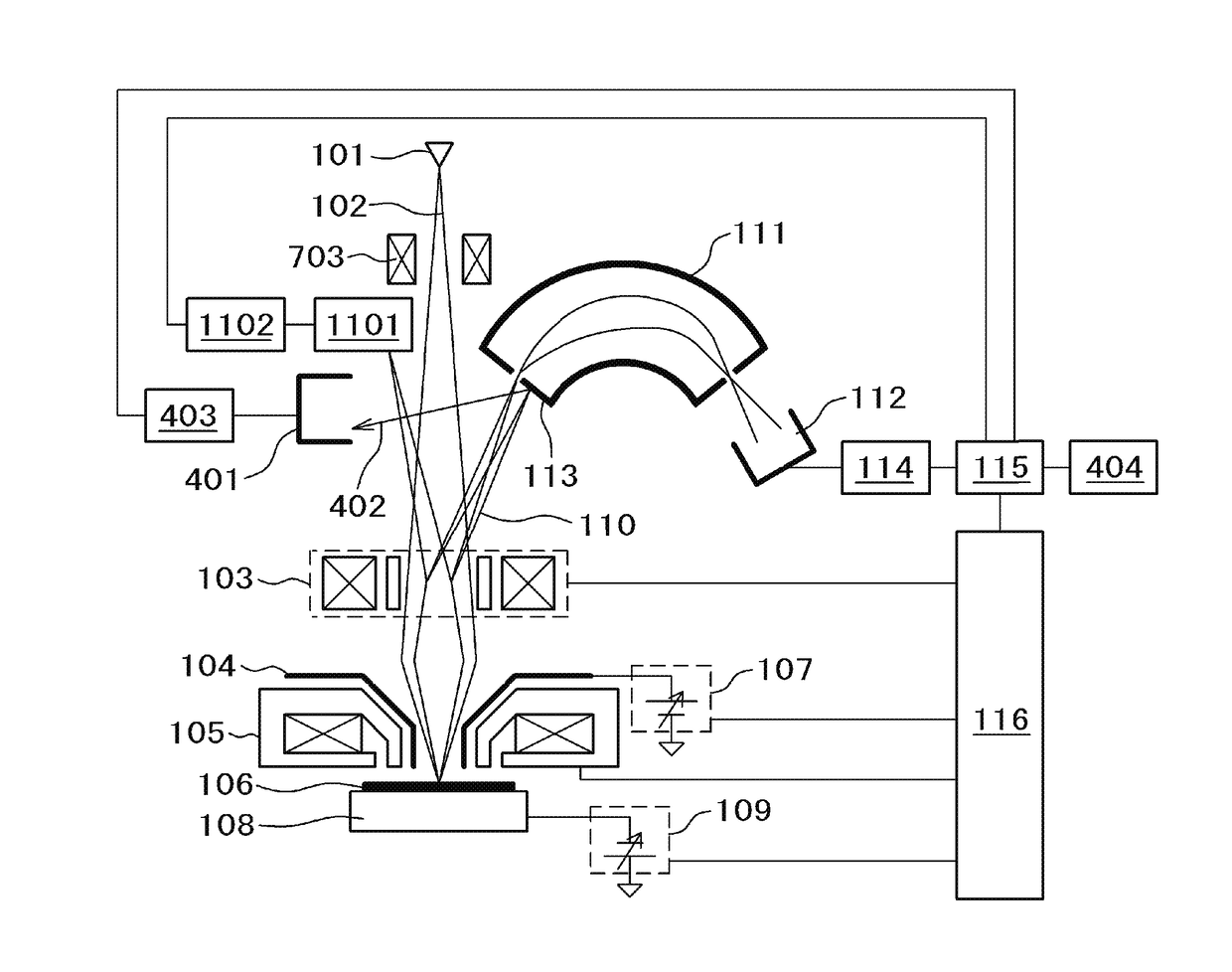
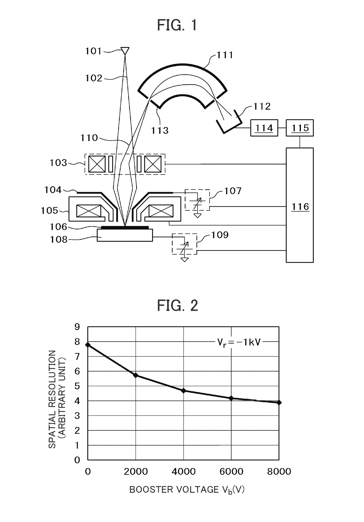
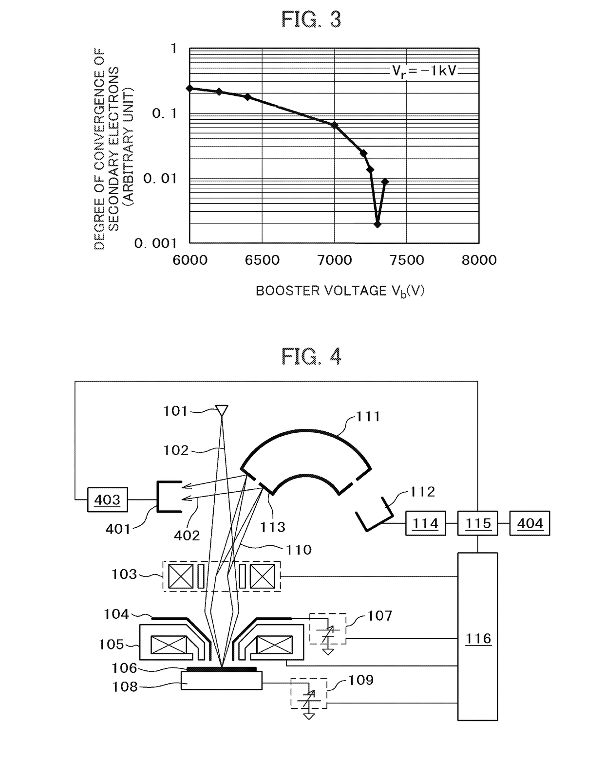
[0053]A first embodiment of the present invention will be described using FIG. 1 to FIG. 3. FIG. 1 is a diagram showing the configuration of an SEM according to the present embodiment. In FIG. 1, primary electrons 102 generated with an electron source 101, pass through a secondary electron deflector 103, then pass through a booster electrode 104 for acceleration of the primary electrons and an objective lens 105, and irradiated to a sample 106. Note that positive polarity voltage is applied from a booster power source 107 to a booster electrode 104. In the electric fields caused with the booster electrode 104, an electric field formed at an end on the sample side is overlapped with a magnetic field caused with the objective lens 105. Hereinbelow, Vb(>0) holds as the voltage applied from the booster power source 107.

[0054]In the present embodiment, an example using, as the configuration of the objective lens 105, a snorkel type objective lens in which the magnetic field of the object...

second embodiment

[0066]A second embodiment of the present invention will be described using FIG. 4 to FIG. 6. Note that the matter described in the first embodiment but not described in the present embodiment is applicable to the present embodiment unless there are special circumstances.

[0067]FIG. 4 is a diagram showing the configuration of the SEM according to the present embodiment. In the present embodiment, a second detector 401, a second signal processor 403 and an image processor 404 are added to the configuration of the first embodiment shown in FIG. 1. The second detector 401 is installed on the opposite side to the spectroscope 111 with the optical axis of the primary electrons 102 between them. The second detector 401 detects first tertiary electrons 402 caused by collision of the secondary electrons 110 against the entrance slit 113. The signal from the second detector 401 is displayed on the display unit 115 through the second signal processor 403 to allow the user to check.

[0068]In the ...

third embodiment

[0073]A third embodiment of the present invention will be described using FIG. 7 to FIG. 11. Note that the matter described in the first or second embodiment but not described in the present embodiment is applicable to the present embodiment unless there are special circumstances.

[0074]FIG. 7 is a diagram showing the configuration of the SEM according to the present embodiment. In the present embodiment, a conversion plate 701 and a deflector 703 to deflect the primary electrons 102 are added to the configuration of the second embodiment shown in FIG. 4. The conversion plate 701 is installed on the opposite side to the spectroscope 111 with the optical axis of the primary electrons 102 between them. The conversion plate generates second tertiary electrons 702 when the secondary electrons 110 collide against it. The second tertiary electrons 702 are detected with the second detector 401 as in the case of the first tertiary electrons 402. The deflector 703 scans the primary electrons ...


PUM


Abstract

To provide a scanning electron microscope having an electron spectroscopy system to attain high spatial resolution and a high secondary electron detection rate under the condition that energy of primary electrons is low, the scanning electron microscope includes: an objective lens 105; primary electron acceleration means 104 that accelerates primary electrons 102; primary electron deceleration means 109 that decelerates the primary electrons and irradiates them to a sample 106; a secondary electron deflector 103 that deflects secondary electrons 110 from the sample to the outside of an optical axis of the primary electrons; a spectroscope 111 that disperses secondary electrons; and a controller that controls application voltage to the objective lens, the primary electron acceleration means and the primary electron deceleration means so as to converge the secondary electrons to an entrance of the spectroscope.

Description

TECHNICAL FIELD[0001]The present invention relates to a scanning electron microscope (hereinbelow SEM) having an electron spectroscopy system and its electron orbit control method.BACKGROUND ART[0002]Currently, the SEM is widely used for observation of a sample having a size ranging from submicron order to nanometer order. The SEM forms an image by irradiating a sample with primary electrons emitted from an electron source while scanning the primary electrons, and detecting secondary electrons caused in the sample. Note that the secondary electrons are divided into “true” secondary electrons characterized in that they have energy equal to or lower than 50 eV and backscattered electrons having energy about the same as incident energy of the primary electrons. A contrast image reflecting the shape of pattern surface, the potential, the difference in work function and the like is obtained from the “true” secondary electrons. On the other hand, a contrast image reflecting the difference...

Claims


Application Information

Patent Timeline
IPC IPC(8): H01J37/26H01J37/147H01J37/10H01J37/285H01J37/28H01J37/05
CPCH01J37/263H01J37/28H01J37/05H01J37/10H01J37/285H01J2237/2823H01J2237/0473H01J2237/0475H01J2237/057H01J2237/1534H01J2237/2806H01J37/1472H01J37/21H01J37/244H01J2237/24485
Inventor BIZEN, DAISUKEMORISHITA, HIDEOHATANO, MICHIOOHTA, HIROYA
Owner HITACHI HIGH-TECH CORP
Why Eureka
Try Eureka