Method for laminating glass panels and vacuum lamination device using same

a vacuum lamination and glass panel technology, applied in the direction of lamination ancillary operations, applications, chemistry apparatus and processes, etc., can solve the problems of affecting the performance of displaying, large deviation from the desired assembling precision, and large precision, so as to reduce manufacturing costs and improve manufacturing yield

Inactive Publication Date: 2017-12-07
TCL CHINA STAR OPTOELECTRONICS TECH CO LTD
View PDF3 Cites 0 Cited by
  • Summary
  • Abstract
  • Description
  • Claims
  • Application Information

AI Technical Summary

Benefits of technology

[0013]An object of the present invention is to provide a method for laminating glass panels, in which a glass panel lamination process and a UV curing process are combined together to effectively improve the yield rate of manufacturing and lower down the cost of manufacturing.
[0014]Another object of the present invention is to provide a vacuum lamination device that has a simple structure and a low cost and can effectively improve the manufacturing efficiency and yield rate of liquid crystal display panel.
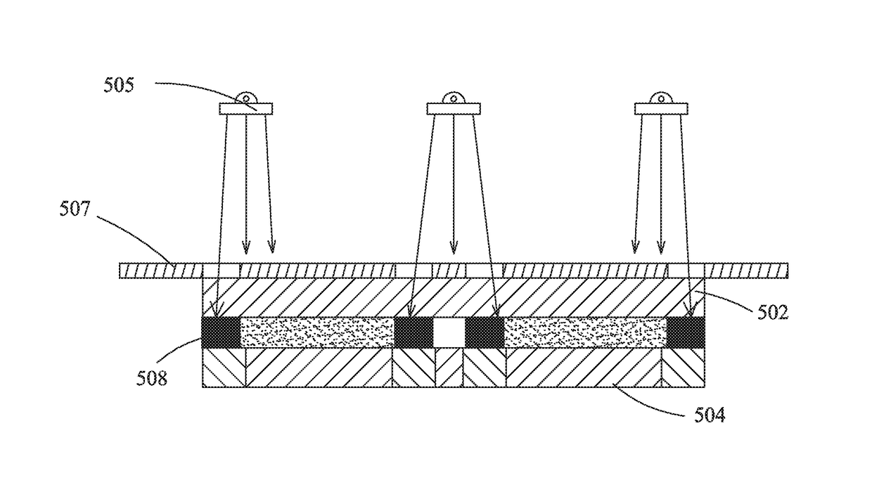
[0034]The efficacy of the present invention is that the present invention provides a method for laminating glass panels and a vacuum lamination device using the method, which effectively lowers down the manufacture cost and improve the yield rate, wherein specifically, a UV lamp module is arranged under a lower positioning plate of the vacuum lamination device to directly irradiate UV light after vacuum lamination of the CF substrate and the TFT substrate in order to cure the seal resin to thereby eliminate the occurrence of downgrading or disposal of product in the conventional process where laminated CF substrate and TFT substrate must be removed out and subjected to turning over, which leads to deformation of the substrates, before UV irradiation can be performed and also effectively shorten the time between lamination and irradiation of UV light to thereby avoid the occurrence of contamination of the liquid crystal by the seal resin or penetration of the liquid crystal through the seal resin due to an excessively long time interval between the two processes. Further, with the arrangement of a prism plate to subject the UV light to filtration, the light that is projected to the TFT substrate is substantially perpendicular to the TFT substrate so as to avoid irradiation of liquid crystal around a seal resin by the UV light due to inappropriate arrangement of sizes and locations of openings of a UV mask and reaction resulting therefrom, which lead to incapability of obtaining a desired pre-tilt angle for alignment operation of liquid crystal in the subsequent process and thus abnormal alignment of the product.

Problems solved by technology

(1) After the TFT substrate and the CF substrate have been laminated but before they are subjected to the irradiation of the UV light, since the seal resin has not yet been cured, turning over may result in a great deviation from the desired assembling precision due to the deformation of the substrates, so that the lamination precision may get larger than 5 um after the irradiation of the UV light and eventually, downgrading or disposal of the product ma result.
(2) Similarly, after the TFT substrate and the CF substrate have been laminated but before they are subjected to the irradiation of the UV light, since the seal resin has not yet been cured, if it would be of a long time (generally around 10 minutes) not subjecting to UV irradiation, molecules of the seal resin may get into the liquid crystal to cause contamination and affecting the performance of displaying; if the time is further extended, then the liquid crystal may penetrate through the seal resin to cause disposal of product, this generally occurring in abnormality of transporting device or malfunctioning of UV irradiating facility.
(3) Irradiation carried out with the UV irradiating facility is generally non-parallel light irradiation so that if size and location of an opening formed in a UV mask are not correct, then liquid crystal located around the seal resin may get exposed to irradiation of the UV light and reaction occurs. This makes it difficult to get a desired pre-tilt angle in a liquid crystal alignment step in the subsequent manufacturing process and leads to alignment abnormality of the product.

Method used

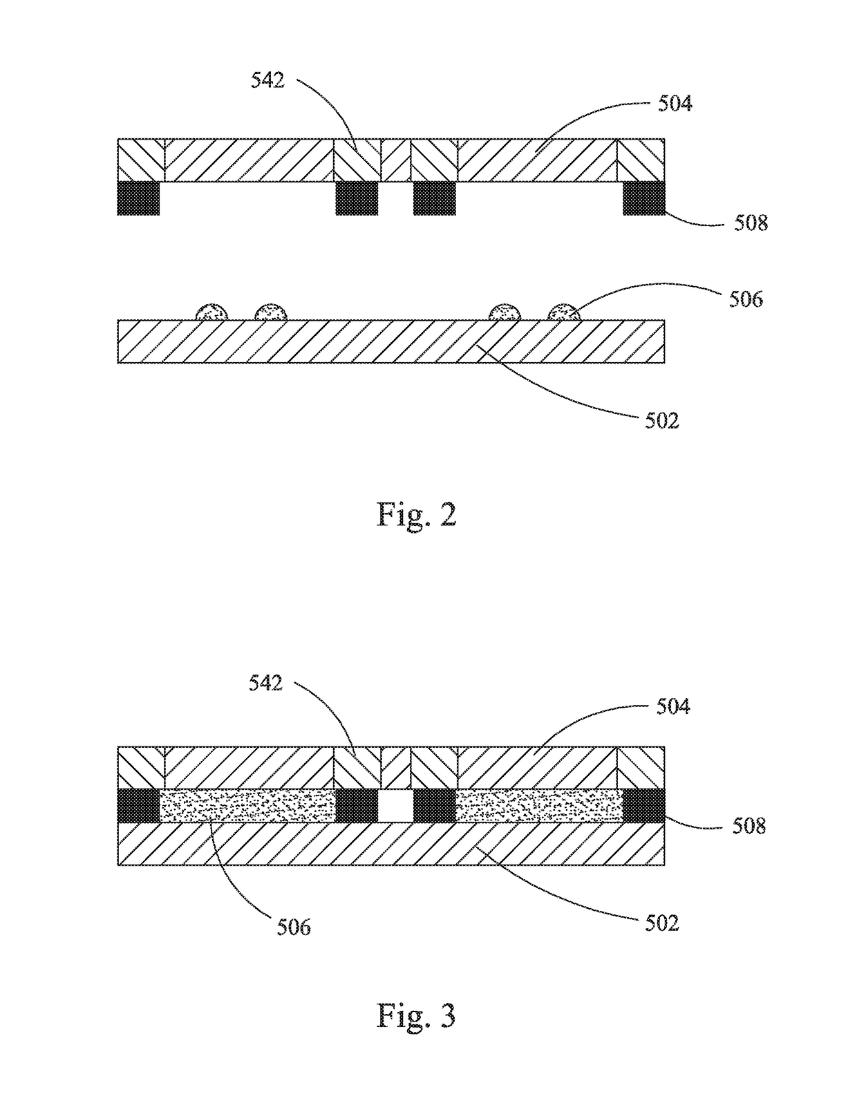

Image

  • Method for laminating glass panels and vacuum lamination device using same
  • Method for laminating glass panels and vacuum lamination device using same
  • Method for laminating glass panels and vacuum lamination device using same

Examples


Embodiment Construction

[0041]To further expound the technical solution adopted in the present invention and the advantages thereof, a detailed description is given to a preferred embodiment of the present invention and the attached drawings.

[0042]Referring to FIG. 6, with additional reference to FIG. 7, the present invention provides a method for laminating glass panels, which specifically comprises the following steps:

[0043]Step 1: providing a TFT (Thin-Film Transistor) substrate 240 and a CF (Color Filter) substrate 220 to be laminated, the CF substrate 220 being coated with a seal resin 204, the TFT substrate 240 carrying liquid crystal 402 dropped thereon.

[0044]Step 2: aligning and laminating the TFT substrate 240 and the CF substrate 220 in a vacuum environment to complete a lamination process.

[0045]Step 2 specifically comprises: providing a vacuum chamber 2, an upper positioning plate 22, and a lower positioning plate 24, wherein the lower positioning plate 24 is made of quartz glass, attracting and...


PUM

PropertyMeasurementUnit
transmittanceaaaaaaaaaa
areaaaaaaaaaaa

Abstract

A method for laminating glass panels includes (1) providing a TFT substrate and a CF substrate to be laminated, in which the CF substrate is coated with a seal resin and the TFT substrate carries liquid crystal dropped thereon; (2) aligning and laminating the TFT substrate and the CF substrate in a vacuum environment to complete a lamination process; (3) applying UV light to transmit through the TFT substrate for carrying out UV curing of the seal resin interposed between the CF substrate and the TFT substrate so as to complete a UV curing process; and (4) removing the laminated CF substrate and the TFT substrate that have been subjected to the UV curing process out of the vacuum environment.

Description

CROSS REFERENCE TO RELATED APPLICATIONS[0001]This is a divisional application of co-pending patent application Ser. No. 14 / 235,071, filed on Aug. 11, 2014, which is a national stage of PCT Application Number PCT / CN2013 / 079968, filed on Jul. 24, 2013, claiming foreign priority of Chinese Patent Application Number 201310293719.4, filed on Jul. 12, 2013.BACKGROUND OF THE INVENTION1. Field of the Invention[0002]The present invention relates to the field of liquid crystal panel manufacturing, and in particular to a method for laminating glass panels and a vacuum lamination device using the method.2. The Related Arts[0003]Liquid crystal displays have a variety of advantages, such as thin device body, low power consumption, and being free of radiation, and are thus of wide applications, such as mobile phone, personal digital assistant (PDA), digital camera, computer monitor, and notebook computer screen.[0004]Most of the liquid crystal displays that are currently available in the market ar...

Claims


Application Information

Patent Timeline
Patent Type & Authority Applications(United States)
IPC IPC(8): H01L21/67B32B38/18B32B37/10B32B38/00
CPCB32B2309/68B32B38/1841B32B2457/202B32B2310/0831B32B2038/0076B32B2037/1063H01L21/67115B32B37/1018B32B17/10954B32B17/06B32B17/10706B32B17/10972B32B7/12
Inventor MA, TAOSONG, TAOLIU, MINGZHAO, GUODONG
Owner TCL CHINA STAR OPTOELECTRONICS TECH CO LTD
Why Eureka
Try Eureka