Method for reducing n-type finfet source and drain resistance

a technology of n-type finfet and drain resistance, applied in the field of reducing integrated circuit package structure and manufacturing, can solve the problems of reducing the performance of finfet devices more severely, adverse device performance effects, etc., to reduce the n-type finfet source and drain resistance, reduce extension resistance, and reduce diffusion

Active Publication Date: 2017-12-07
SEMICON MFG INT (SHANGHAI) CORP +1
View PDF0 Cites 11 Cited by
  • Summary
  • Abstract
  • Description
  • Claims
  • Application Information

AI Technical Summary

Benefits of technology

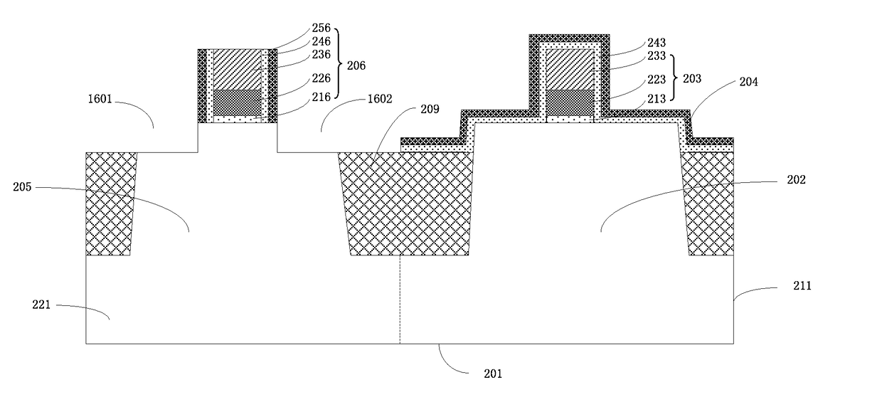
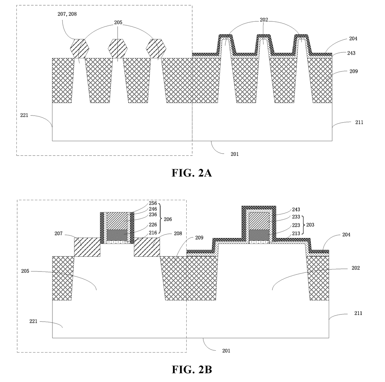
[0022]Some embodiments of the invention can reduce n-type FinFET source and drain resistance. For example, after n-type source / drain formation, the first phosphorus implant is to reduce extension resistance, and is implanted post LDD spike anneal and SiGe epitaxial growth process in the PMOS region, in order to reduce diffusion during thermal processes, which will lead to a worse short channel effect. The source / drain recessed regions are implemented to provide a larger volume for epitaxy growth, which will bring more stress into the channel, and improve device performance. The silicon epitaxial growth in the n-type source and drain includes heavy in-situ implantation with a phosphorus dose as high as 1×10²¹ / cm3. Next, a phosphorus implant is carried out to reduce the Schottky barrier height, which will reduce the contact resistance.

Problems solved by technology

High resistance in the source and drain regions can have adverse effects in device performance, particularly in FinFET devices.
Due to the smaller size, the high resistance of the source and drain regions will reduce the performance of FinFET devices more severely.

Method used


Image

  • Method for reducing n-type finfet source and drain resistance
  • Method for reducing n-type finfet source and drain resistance
  • Method for reducing n-type finfet source and drain resistance

Examples


Embodiment Construction

[0027]The drawings of various exemplary embodiments of the present invention will be described in detail. It should be noted that, unless otherwise specified, the relative arrangement set forth in these embodiments, components and steps, the numerical expressions, and values do not limit the scope of the present invention. At the same time, it should be appreciated that, for ease of description, the dimensions of the various parts are not illustrated in the drawings according to the actual proportional relationship.

[0028]The following description of exemplary embodiments is merely illustrative of the present invention and in no way intends to impose any restrictions on its use or application. Techniques, methods, and equipment known to someone of ordinary skill in the relevant art may not be discussed in detail, but in appropriate cases, the techniques, methods and equipment should be considered as part of the specification.

[0029]In all the examples shown and discussed, any specific...


PUM


Abstract

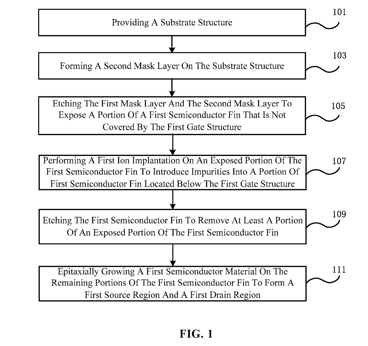
A method of manufacturing a semiconductor device includes providing a substrate structure, the substrate structure having a semiconductor substrate including a first semiconductor fin, a first gate structure, and a first mask layer on a first semiconductor region. The method includes forming a second mask layer on the substrate structure, etching first mask layer and second mask layer to expose a portion of a first semiconductor fin not covered by the first gate structure, performing a first ion implantation on an exposed portion of the first semiconductor fin to introduce impurities into a portion of the first semiconductor fin located below the first gate structure, etching the first semiconductor fin to remove a portion of an exposed portion of the first semiconductor fin, and epitaxially growing a first semiconductor material on the remaining portions of the first semiconductor fin to form a first source region and a first drain region.

Description

CROSS-REFERENCES TO RELATED APPLICATIONS[0001]This application claims priority to Chinese patent application No. 201610379189.9, filed on Jun. 1, 2016, the content of which is incorporated herein by reference in its entirety.BACKGROUND OF THE INVENTION[0002]The present invention relates to the field of semiconductor technology. Embodiments of the invention relate to integrated circuit package structures and manufacturing methods.[0003]In FinFET (Fin Field Effect Transistor) devices, the parasitic resistance has a great influence on the resistance of the source region and the drain region. The parasitic resistance can be caused by a variety of reasons. For example, an important contribution to the parasitic resistance comes from the contact resistance between a metal silicide and the source and drain regions. And the contact between metal silicides with the source and drain regions tends to pinch the Fermi level near the middle of the band gap, which leads to a large Schottky barrier...

Claims


Application Information

Patent Timeline
Patent Type & Authority Applications(United States)
IPC IPC(8): H01L21/8234H01L29/66H01L29/06H01L27/088H01L21/311H01L21/308H01L21/268H01L21/265H01L21/263H01L29/78H01L21/02
CPCH01L21/823431H01L29/785H01L29/66795H01L29/66492H01L29/0649H01L27/0886H01L21/823437H01L21/0257H01L21/3081H01L21/268H01L21/26586H01L21/26513H01L21/2636H01L21/31144H01L29/0847H01L21/823821H01L29/66803H01L29/7848
Inventor LI, YONG
Owner SEMICON MFG INT (SHANGHAI) CORP
Why Eureka
Try Eureka