Method of processing a wafer and wafer processing system

a processing system and wafer technology, applied in the field of processing a wafer, can solve the problems of increasing processing costs, laborious and time-consuming, and restricting the choice of possible tape materials, and achieves stable and reliable fixation of adhesive tape, good access, and efficient and accurate manner.

Active Publication Date: 2017-12-21
DISCO CORP
View PDF4 Cites 4 Cited by
  • Summary
  • Abstract
  • Description
  • Claims
  • Application Information

AI Technical Summary

Benefits of technology

[0014]Hence, the second annular frame can be attached to the peripheral portion of the expanded adhesive tape in a simple manner, reliably maintaining radial tension of the tape and thus preventing any damage to the dies due to an unintentional contact therebetween.
[0082]The wafer processing system may comprise three or more wafer processing apparatuses connected to each other. One of the wafer processing apparatuses may comprise the support member and the first and second frame holding means. The other wafer processing apparatuses may each comprise a laser beam applying means. In this case, a single support member and single first and second frame holding means may be used for, i.e., in combination with, a plurality of, e.g., two or three, laser beam applying means, thus significantly reducing the equipment costs.

Problems solved by technology

However, the approach taught in DE 10 2010 046 665 A1 requires the preparation of an annular frame with a suitably adapted ring-shaped tape attached thereto and is thus laborious and time-consuming.
Since the tape has to be cut into an appropriate ring shape, there are significant material losses, resulting in increased processing costs.
Also, the characteristics of the ring-shaped tape have to be precisely matched with those of the expandable tape, thus restricting the choice of possible tape materials.
Further, the tension of the ring-shaped tape may decrease over time, creating the risk of unintentional contact between the dies, e.g., during storage or shipping thereof.

Method used


Image

  • Method of processing a wafer and wafer processing system
  • Method of processing a wafer and wafer processing system
  • Method of processing a wafer and wafer processing system

Examples


first embodiment

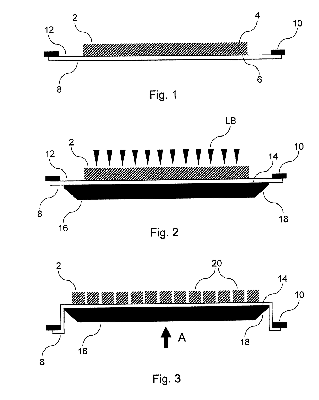
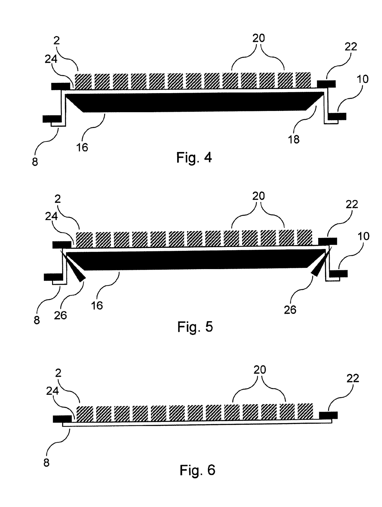
[0106]In the following, the method of processing a wafer of the present invention and of the wafer processing system of the present invention will be described with reference to FIGS. 1 to 6.

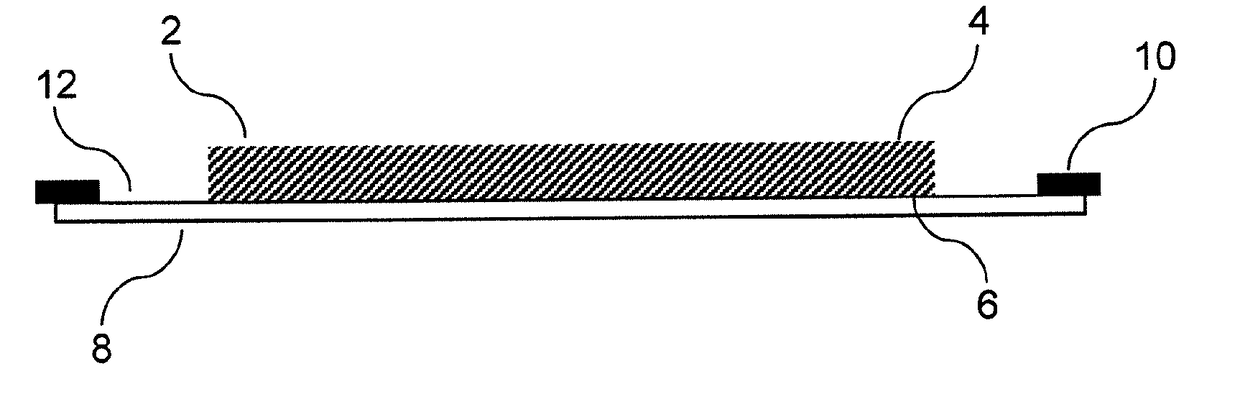
[0107]As is shown in FIG. 1, the wafer 2 to be processed by the method of the invention has a front side 4 and a back side 6 opposite to the front side 4. A device area (not shown) with a plurality of devices partitioned by a plurality of division lines (not shown) is formed on the front side 4 of the wafer 2.

[0108]The wafer 2 may be, for example, a semiconductor wafer, a glass wafer, a sapphire wafer, a ceramic wafer, such as an alumina (Al2O3) ceramic wafer, a silicon oxide (SiO2) wafer, an aluminium nitride (AlN) wafer or the like.

[0109]In particular, the wafer 2 may be, for example, a silicon (Si) wafer, a gallium arsenide (GaAs) wafer, a gallium nitride (GaN) wafer, a gallium phosphide (GaP) wafer, an indium arsenide (InAs) wafer, an indium phosphide (InP) wafer, a silicon carbide (SiC) waf...

second embodiment

[0132]In the following, the method of processing a wafer of the present invention and of the wafer processing system of the present invention will be described with reference to FIGS. 7 to 11.

[0133]The second embodiment of the invention substantially differs from the first embodiment of the invention in the configuration of the support member 16, as will be detailed below. In the description of the second embodiment, those elements which are substantially identical to those of the first embodiment are denoted by the same reference signs and a repeated description thereof is omitted.

[0134]As is shown in FIG. 7, the support member 16 according to the second embodiment comprises a central part 16a and an annular peripheral part 16b surrounding the central part 16a. The peripheral part 16b of the support member 16 is movable relative to the central part 16a of the support member 16 in the direction perpendicular to the plane of the support surface 14.

[0135]The central part 16a is in the...


PUM

PropertyMeasurementUnit
inner diameteraaaaaaaaaa
thicknessaaaaaaaaaa
thicknessaaaaaaaaaa

Abstract

A wafer has a device area on one side with a plurality of devices partitioned by a plurality of division lines. Either side of the wafer is attached to an adhesive tape supported by a first annular frame. A modified region is formed in the wafer along the division lines by a laser. The wafer is placed on a support member whose outer diameter is smaller than an inner diameter of the first annular frame. After applying the laser beam, the adhesive tape is expanded thereby dividing the wafer along the division lines. A second annular frame is attached to a portion of the expanded adhesive tape. An inner diameter of the second annular frame is smaller than the outer diameter of the support member and smaller than the inner diameter of the first annular frame.

Description

TECHNICAL FIELD[0001]The present invention relates to a method of processing a wafer, having on one side a device area with a plurality of devices partitioned by a plurality of division lines. Further, the invention relates to a wafer processing system for carrying out this method.TECHNICAL BACKGROUND[0002]In a semiconductor device fabrication process, a wafer having a device area with a plurality of devices partitioned by a plurality of division lines is divided into individual dies or chips along the division lines.[0003]Substantially the same approach as detailed above is also adopted to obtain, for example, individual power devices, optical devices, medical devices, electrical components or MEMS devices from wafers with device areas, in which these devices are formed.[0004]In order to reduce the strength of the wafer along the division lines prior to dividing the wafer, it is known to form a modified region in the wafer along the division lines. This modified region may be in th...

Claims


Application Information

Patent Timeline
Patent Type & Authority Applications(United States)
IPC IPC(8): H01L21/8222B28D5/00B23K26/364B23K26/08H01L27/01H01L21/76
CPCH01L21/8222H01L27/01B23K26/364B23K26/083B28D5/0029H01L21/76B23K26/0006B28D5/0011B23K26/08B28D5/0082B23K26/402B23K26/359B23K26/0622B23K2101/40B23K2103/50B23K2103/52H01L21/78H01L21/67132
Inventor PRIEWASSER, KARLHOSHINO, HITOSHI
Owner DISCO CORP
Why Eureka
Try Eureka