
Method for coating devices and resulting products

a technology of nanoparticles and coatings, applied in the direction of dielectric characteristics, non-metallic protective coating applications, printed circuit board assemblies (pcba) with electronic components thereon, etc., can solve the problems of easy thickness of protective film too thick or with non-uniform distribution, and uneven thickness of protective film, etc., to achieve good waterproof effect, less friction or other functions, and thin thickness

Active Publication Date: 2017-12-21
NANO SHIELD TECH CO LTD
View PDF2 Cites 5 Cited by
  • Summary
  • Abstract
  • Description
  • Claims
  • Application Information

AI Technical Summary

Benefits of technology

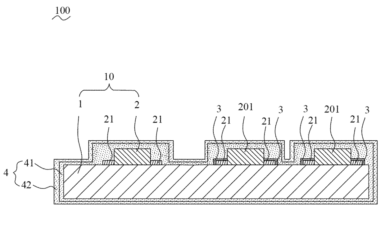
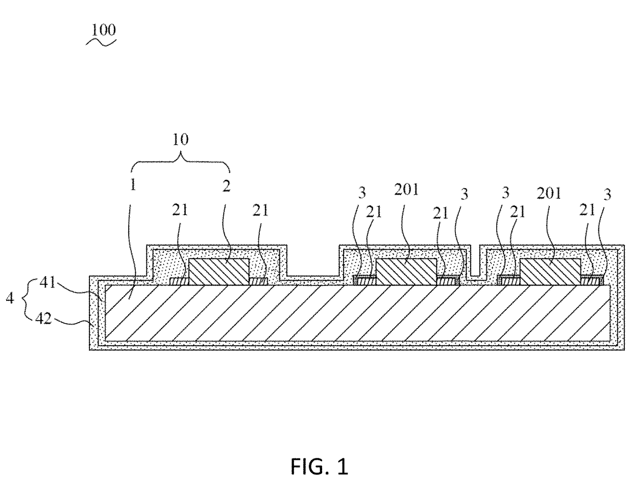
The device is coated with a waterproof coating and a nanofilm made of metal oxide nanoparticles and silicon dioxide nanoparticles. This coating and nanofilm make the device resistant to water and provide a smooth surface. The nanofilm can also reduce friction and perform other functions. The nanofilm is thin and uniform, and made up of nanoparticles that are smaller than the metal oxide nanoparticles.

Problems solved by technology

With the progress of a large variety of technologies, many electronic components have developed gradually along the microminiaturization and the diversification, and a design of a printed circuit board assembly (PCBA) with the electronic components thereon is more complex.
However, a prior art technology usually uses a coating process to protect the PCBA and the other devices, but the traditional coating process is easy to make a thickness of the protective film too thick or with non-uniform distribution.
Another prior art technology employs a vapor deposition process to form the protective film on the PCBA, but the vapor deposition process often makes the protective film not be uniform because of placed angles of the electronic components.

Method used


Image

  • Method for coating devices and resulting products
  • Method for coating devices and resulting products
  • Method for coating devices and resulting products

Examples


examples

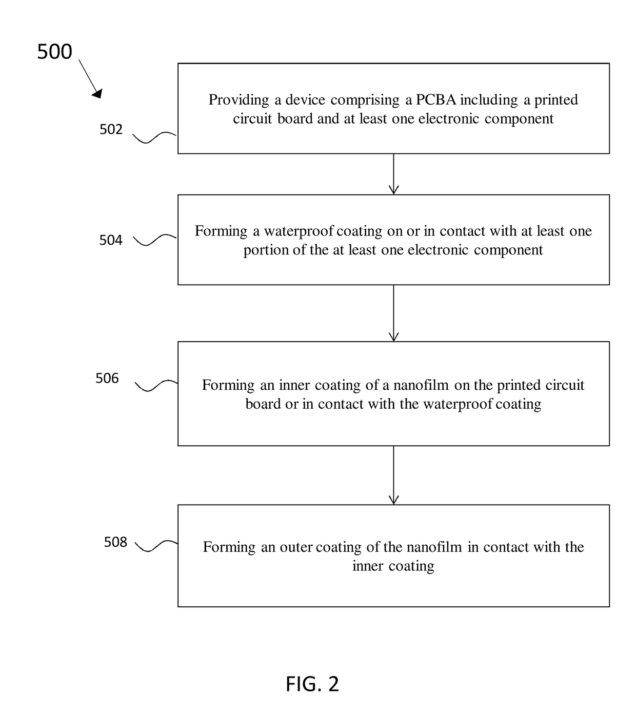
[0058]Nanofilm coatings were formed using the following two solutions (or mixtures or suspensions) after a waterproof polymer coating is formed. For example, the polymer coating can be formed by UV curing a cross linkable composition (e.g., Seal-glo 602 MCF) or by coating a silicone material (e.g., silicone 380B).

[0059]In the embodiments listed described below, the first solution comprises TiO2 nanoparticles and the second solution comprises SiO2 nanoparticles. The content of TiO2 nanoparticles in the first solution is dispersed in the pure water which in a range from about 0.8 wt. % to about 1.5 wt. %. The first solution has a density of 1.01 g / cm3. The content of SiO2 nanoparticles in the second solution is dispersed in heptane, cetane and methyl hydrogen siloxane (about 0.1-5 wt. %), which is in a range from about 0.3 wt. % to about 5 wt. %. The second solution has a density of 0.774 g / cm3. For example, in one exemplary process embodiment, a PCBA was coated with a polymer coating...


PUM

PropertyMeasurementUnit
particle diameteraaaaaaaaaa
temperatureaaaaaaaaaa

Abstract

A method for waterproofing a device and the resulting device are provided. The device includes a printed circuit board assembly (PCBA), which includes a printed circuit board, and at least one electronic component disposed on the printed circuit board. A waterproof coating such as a polymer coating is disposed on or in contact with at least one portion of the at least one electronic component. A nanofilm is disposed on the PCBA. The nanofilm includes an inner coating and an outer coating. The inner coating is disposed on the printed circuit board or in contact with the waterproof coating. The inner coating comprises metal oxide nanoparticles having a particle diameter in a range of about 5 nm to about 100 nm. The outer coating in contact with the inner coating, and comprises silicon dioxide nanoparticles having a particle diameter in a range of 0.1 nm to 10 nm.

Description

PRIORITY CLAIM AND CROSS-REFERENCE[0001]The present application is based upon and claims priority to U.S. Provisional Application No. 62 / 351,590 filed Jun. 17, 2016, U.S. Provisional Application No. 62 / 357,550 filed Jul. 1, 2016, and U.S. Provisional Application No. 62 / 367,838 filed Jul. 28, 2016, all of which are expressly incorporated by reference herein in their entireties.FIELD OF THE INVENTION[0002]The disclosed subject matter generally relates to a method for coating a device, and more particularly to a method for coating a device with nanoparticles, and the resulting coated device.BACKGROUND[0003]With the progress of a large variety of technologies, many electronic components have developed gradually along the microminiaturization and the diversification, and a design of a printed circuit board assembly (PCBA) with the electronic components thereon is more complex. Therefore, it is important to decide what way to protect the PCBA from being moistened by some exterior chemical...

Claims


Application Information

Patent Timeline
Patent Type & Authority Applications(United States)
IPC IPC(8): H05K3/28H05K1/18H05K3/30
CPCH05K3/284H05K1/185H05K2201/0104H05K2201/015H05K2201/0158H05K3/303H05K3/285H05K2201/0195H05K2201/0179H05K2201/0257H05K2203/1333H05K3/282B05D5/00B05D7/24B05D3/0254
Inventor LEE, JAMES CHENG
Owner NANO SHIELD TECH CO LTD
Learn More