Method for fabricating flexible substrate

a technology of flexible substrates and substrates, which is applied in the manufacture of cable/conductors, conductive layers on insulating supports, synthetic resin layered products, etc., can solve the problems of low productivity, low process complexity, and limit the choice of materials, so as to reduce production cost and time, simplify the production process, and facilitate separation

Active Publication Date: 2017-12-28
LG CHEM LTD
View PDF3 Cites 15 Cited by
  • Summary
  • Abstract
  • Description
  • Claims
  • Application Information

AI Technical Summary

Benefits of technology

[0045]According to the method of the present invention, a flexible substrate can be continuously produced based on a roll-to-roll process, and at the same time, a flexible substrate layer can be easily separated from a carrier substrate by the application of a relatively small physical stimulus without involving laser or light irradiation or dissolution. Therefore, the method of the present invention enables the production of a flexible substrate for use in an electronic device, such as a flexible display device, in an easier manner and the production process can be simplified. In addition, the production cost and time can be reduced. The device of the present invention can be prevented from deterioration of reliability and occurrence of defects caused by laser or light irradiation.
[0046]According to the method of the present invention, since a flexible substrate is obtained by separating a flexible substrate layer supported on a carrier substrate, a force applied to the flexible substrate along the machine direction is not substantially different from that along the transverse direction, and as a result, the flexible substrate has uniform mechanical, thermal, and optical properties without significant differences in the machine and transverse directions.
[0047]According to the method of the present invention, a flexible substrate with metal wires can be obtained in the form of a roll. The use of the flexible substrate increases the efficiency of a subsequent process for fabricating an electronic device, enabling more efficient fabrication of an electronic device.

Problems solved by technology

This process is complicated and has low productivity.
For approach (1), however, resistivity limits the choice of materials.
Other materials, such as silver, are only available at high prices, limiting their use.
Approach (2) is physically limited due to problems associated with circuit design.
However, as the height of wires increases, many problems may arise, for example, disordered alignment of the wires, electrical shorting, short circuiting between the wires, and damage to the wires.
However, such conventional techniques require the consumption of large amounts of materials by repeated deposition / etching, involve complicated processing steps, and cause thermal damage to a plastic substrate upon thermal treatment of a metal layer formed in the plastic substrate.
However, according to this technique, when the hard substrate is forcibly peeled from the metal wire embedded polymer substrate, damage to the metal wires and the polymer substrate is caused, leading to defects in a final product.
According to this method, however, removal of the sacrificial layer by dissolution in water or an organic solvent or photodecomposition increases the costs associated with the treatment of the water or organic solvent after use.

Method used


Image

  • Method for fabricating flexible substrate
  • Method for fabricating flexible substrate
  • Method for fabricating flexible substrate

Examples


example 1

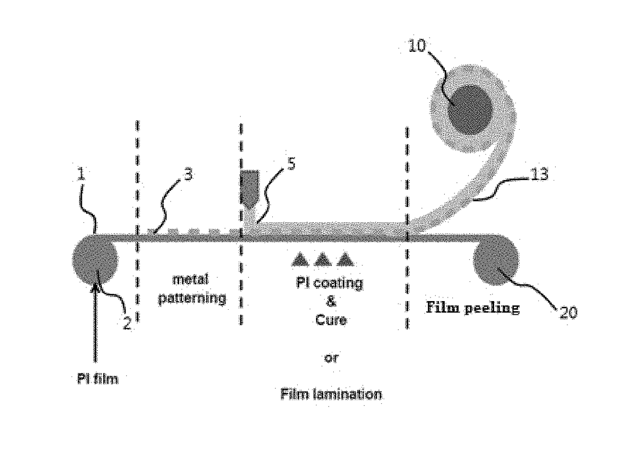
[0133]1 mol of BPDA was polymerized with 0.99 mol of PDA to prepare a polyamic acid resin. A composition including 20 wt % of the polyamic acid resin and 80 wt % of DMAc as a solvent was cast on a support. Thereafter, the coating was continuously dried at a temperature of 120° C. and cured at stepwise increasing temperatures (150° C.→230° C.→300° C.→400° C.) for 30 min to form a 50 μm thick film (carrier substrate) including a polyimide resin in the form of a roll.

[0134]1 mol of BPDA was polymerized with 0.99 mol of TFMB to prepare a polyamic acid resin. 12 wt % of the polyamic acid resin was mixed with 88 wt % of DMAc as a solvent to prepare a composition for the formation of a flexible substrate layer.

[0135]While the carrier substrate was unwound and transferred at a speed of 0.5 m / min, the composition was applied (cast) to the carrier substrate in the form of a roll such that the thickness after drying was 15 μm. The resulting coating was continuously dried at a temperature of 10...

example 2

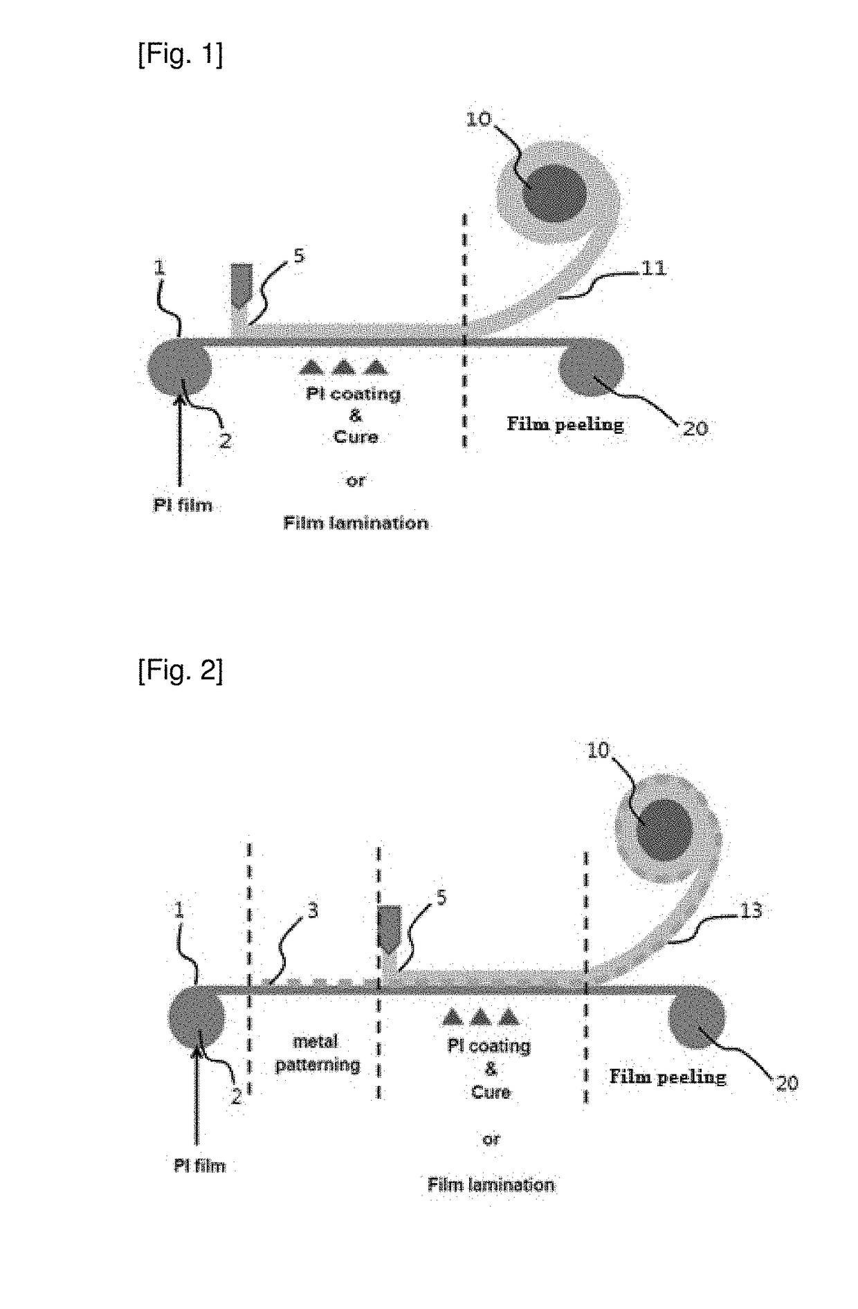
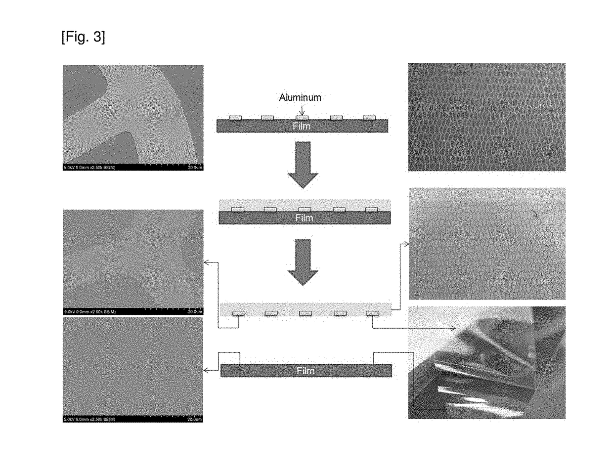
[0142]The procedure of Example 1 was repeated except that aluminum was deposited to a thickness of 200 nm on the carrier substrate and was micropatterned before application of the composition for the formation of a flexible substrate layer to the carrier substrate, as illustrated in FIG. 2. Specifically, a resist ink was coated on the entire surface of a silicone blanket and then a cliche engraved with micropatterns was brought into contact with the blanket to form patterns on the silicone blanket. Subsequently, portions of the coating were removed to form micropatterns on the silicone blanket. The resist ink micropatterns formed on the silicone blanket were transferred to the aluminum-deposited carrier substrate and dried in an oven at 115° C. for 3 min to remove the solvent remaining in the resist patterns. The resist patterned aluminum substrate was etched with an etchant by spraying at 45° C. The etchant was cleaned off with deionized water, followed by drying. The remaining res...


PUM

PropertyMeasurementUnit
adhesion strengthaaaaaaaaaa
peel strengthaaaaaaaaaa
temperatureaaaaaaaaaa

Abstract

The present invention relates to a method for producing a flexible substrate. According to the method of the present invention, a flexible substrate layer can be easily separated from a carrier substrate even without the need for laser or light irradiation so that a device can be prevented from deterioration of reliability and occurrence of defects caused by laser or light irradiation. In addition, according to the method of the present invention, a flexible substrate can be continuously produced in an easier manner based on a roll-to-roll process.

Description

[0001]This application claims the benefit of priority to Korean Patent Application No. 10-2015-0104964, filed on Jul. 24, 2015, the entire disclosure of which is incorporated herein by reference.BACKGROUND OF THE INVENTION1. Field of the Invention[0002]The present invention relates to a method for producing a flexible substrate, and more specifically to a method for more efficiently producing a flexible substrate using a carrier substrate from which the flexible substrate is easy to peel.2. Description of the Related Art[0003]Flexible electronics, for example, flexible displays, solar cells, area lighting devices, e-papers, flexible secondary batteries, and touch panels, have recently received attention as promising technologies.[0004]Flexible electronics have developed to make inexpensive, easy-to-bend, and transparent electronic devices and systems.[0005]According to a conventional process for producing a flexible substrate, a solvent-containing solution for producing a flexible s...

Claims


Application Information

Patent Timeline
Patent Type & Authority Applications(United States)
IPC IPC(8): H05K1/03B32B15/08H05K3/20H05K3/00H05K1/02
CPCH05K1/0393B32B15/08H05K1/0313H05K2203/0264H05K1/0283H05K3/207H05K2201/10128H05K3/0041B32B7/06B32B7/12B32B27/06B32B27/34B32B33/00B32B37/12B32B38/10C08G73/1007C08G73/1067B32B2457/12B32B2457/10B32B2457/20B32B2457/206Y02P20/582H05K1/0346H05K3/20H05K2201/0108H05K2201/0154H05K2201/0317H05K2201/10106H05K2203/0156H05K2203/1545F21K99/00H01B3/30H01B5/14H01B7/04H01B13/00H01L31/0236Y02E10/549H10K71/621H10K77/111H10K30/83H10K50/814H10K50/824F21K9/90H01B13/0026H01L31/02366H10K50/80
Inventor JEONG, HYE WONSON, YONG GOOKIM, KYUNGJUNSHIN, BO RALIM, CHANG YOON
Owner LG CHEM LTD
Why Eureka
Try Eureka