Reducing or avoiding metal deposition from etching magnetic tunnel junction (MTJ) devices, including magnetic random access memory (MRAM) devices

Active Publication Date: 2018-02-08
QUALCOMM INC
View PDF2 Cites 29 Cited by
  • Summary
  • Abstract
  • Description
  • Claims
  • Application Information

AI Technical Summary

Benefits of technology

[0011]Aspects of the present disclosure involve reducing or avoiding metal deposition from etching of magnetic tunnel junction (MTJ) devices. For example, such MTJ devices may be employed to provide resistive memory bit cells for magnetic random access memory (MRAM). In one exemplary aspect disclosed herein, a width of a bottom electrode of an MTJ device is provided to be less than a width of the MTJ stack pillar in the MTJ device. In this manner, when the MTJ device is over-etched to avoid horizontal shorts between an adjacent device(s), etching of the bottom electrode is reduced or avoided to reduce or avoid metal redeposition on the MTJ stack pillar of the MTJ device. In another exemplary aspect disclosed herein, a metal seed layer for providing a textured conductive coupling of an MTJ stack pillar of the MTJ device to a bottom electrode of the MTJ device is embedded in the bottom

Problems solved by technology

At worst, this magnetic field bias can be strong enough to “flip” the value of a memory bit cell employing the pMTJ 200 in FIG. 2, thus decreasing the reliability of the subject MRAM.
Currently known methods for MTJ etching, especially at tight pitches, include ion beam etching (IBE) and chemical etching in a reactive ion etching (RIE), both of which have challenges.
RIE processes are known to create damage zones around the perimeter of

Method used


Image

  • Reducing or avoiding metal deposition from etching magnetic tunnel junction (MTJ) devices, including magnetic random access memory (MRAM) devices
  • Reducing or avoiding metal deposition from etching magnetic tunnel junction (MTJ) devices, including magnetic random access memory (MRAM) devices
  • Reducing or avoiding metal deposition from etching magnetic tunnel junction (MTJ) devices, including magnetic random access memory (MRAM) devices

Examples


Embodiment Construction

[0030]With reference now to the drawing figures, several exemplary aspects of the present disclosure are described. The word “exemplary” is used herein to mean “serving as an example, instance, or illustration.” Any aspect described herein as “exemplary” is not necessarily to be construed as preferred or advantageous over other aspects.

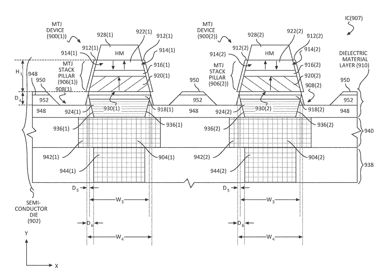
[0031]Aspects of the present disclosure involve reducing or avoiding metal deposition from etching of magnetic tunnel junction (MTJ) devices. For example, such MTJ devices may be employed to provide resistive memory bit cells for magnetic random access memory (MRAM). In one exemplary aspect disclosed herein, a width of a bottom electrode of an MTJ device is provided to be less than a width of the MTJ stack pillar in the MTJ device. In this manner, when the MTJ device is over-etched to avoid horizontal shorts between an adjacent device(s), etching of the bottom electrode is reduced or avoided to reduce or avoid metal redeposition on the MTJ stack pilla...


PUM


Abstract

Aspects disclosed include reducing or avoiding metal deposition from etching magnetic tunnel junction (MTJ) devices. In one example, a width of a bottom electrode of an MTJ device is provided to be less than a width of the MTJ stack of the MTJ device. In this manner, etching of the bottom electrode may be reduced or avoided to reduce or avoid metal redeposition as a result of over-etching the MTJ device to avoid horizontal shorts between an adjacent device(s). In another example, a seed layer is embedded in a bottom electrode of the MTJ device. In this manner, the MTJ stack is reduced in height to reduce or avoid metal redeposition as a result of over-etching the MTJ device. In another example, an MTJ device includes an embedded seed layer in a bottom electrode which also has a width less than a width of the MTJ stack.

Description

PRIORITY CLAIM[0001]The present application claims priority under 35 U.S.C. §119(e) to U.S. Provisional Patent Application Ser. No. 62 / 370,929 filed on Aug. 4, 2016 and entitled “REDUCING OR AVOIDING METAL DEPOSITION FROM ETCHING MAGNETIC TUNNEL JUNCTION (MTJ) DEVICES, INCLUDING MAGNETIC RANDOM ACCESS MEMORY (MRAM) DEVICES,” the contents of which is incorporated herein by reference in its entirety.BACKGROUNDI. Field of the Disclosure[0002]The technology of the disclosure relates generally to magnetic tunnel junction (MTJ) devices, which may be employed in a resistive memory, such as a magnetic random access memory (MRAM) for example, and more particularly to fabrication of MTJ devices.II. Background[0003]Semiconductor storage devices are used in integrated circuits (ICs) in electronic devices to provide data storage. One example of a semiconductor storage device is magnetic random access memory (MRAM). MRAM is non-volatile memory in which data is stored by programming a magnetic tun...

Claims


Application Information

Patent Timeline
IPC IPC(8): H01L27/22H01L43/10G11C11/16H01L43/12H01L43/02H01L43/08
CPCH01L27/228H01L43/02H01L43/10G11C11/161H01L43/12H01L43/08H10B61/22H10N50/10H10N50/01H10N50/80H10N50/85
Inventor PARK, CHANDOKAN, JIMMY JIANANKANG, SEUNG HYUK
Owner QUALCOMM INC
Why Eureka
Try Eureka