Bonded substrate, surface acoustic wave element, surface acoustic wave device, and method of manufacturing bonded substrate

a technology of surface acoustic wave and acoustic wave element, which is applied in the direction of impedence network, electrical apparatus, etc., can solve the problems of poor yield and extremely poor yield of devices having the proposed structure, and achieve excellent yield and high electromechanical coupling factor , the effect of high phase velocity

Active Publication Date: 2018-02-15
JAPAN STEEL WORKS LTD
View PDF0 Cites 14 Cited by
  • Summary
  • Abstract
  • Description
  • Claims
  • Application Information

AI Technical Summary

Benefits of technology

[0062]According to the bonded substrate of the present invention, the quartz substrate and the piezoelectric substrate are bonded in excellent yield. The surface acoustic wave element using this bonded substrate affords a high phase velocity and a high electromechanical coupling factor. Accordingly, a SAW substrate can be produced in which an LLSAW does not suffer from propagation attenuation and the

Problems solved by technology

However, while in Patent Literature 1, it is confirmed that losses caused by bulk wave radiation of an LLSAW are reduced and propagation characteristics and the like are remarkably improved, there is problem that in the yield of devices having the proposed structure is extremely poor.

Method used


Image

  • Bonded substrate, surface acoustic wave element, surface acoustic wave device, and method of manufacturing bonded substrate
  • Bonded substrate, surface acoustic wave element, surface acoustic wave device, and method of manufacturing bonded substrate
  • Bonded substrate, surface acoustic wave element, surface acoustic wave device, and method of manufacturing bonded substrate

Examples


example 1

[0090]Hereafter, an example of the present invention is described.

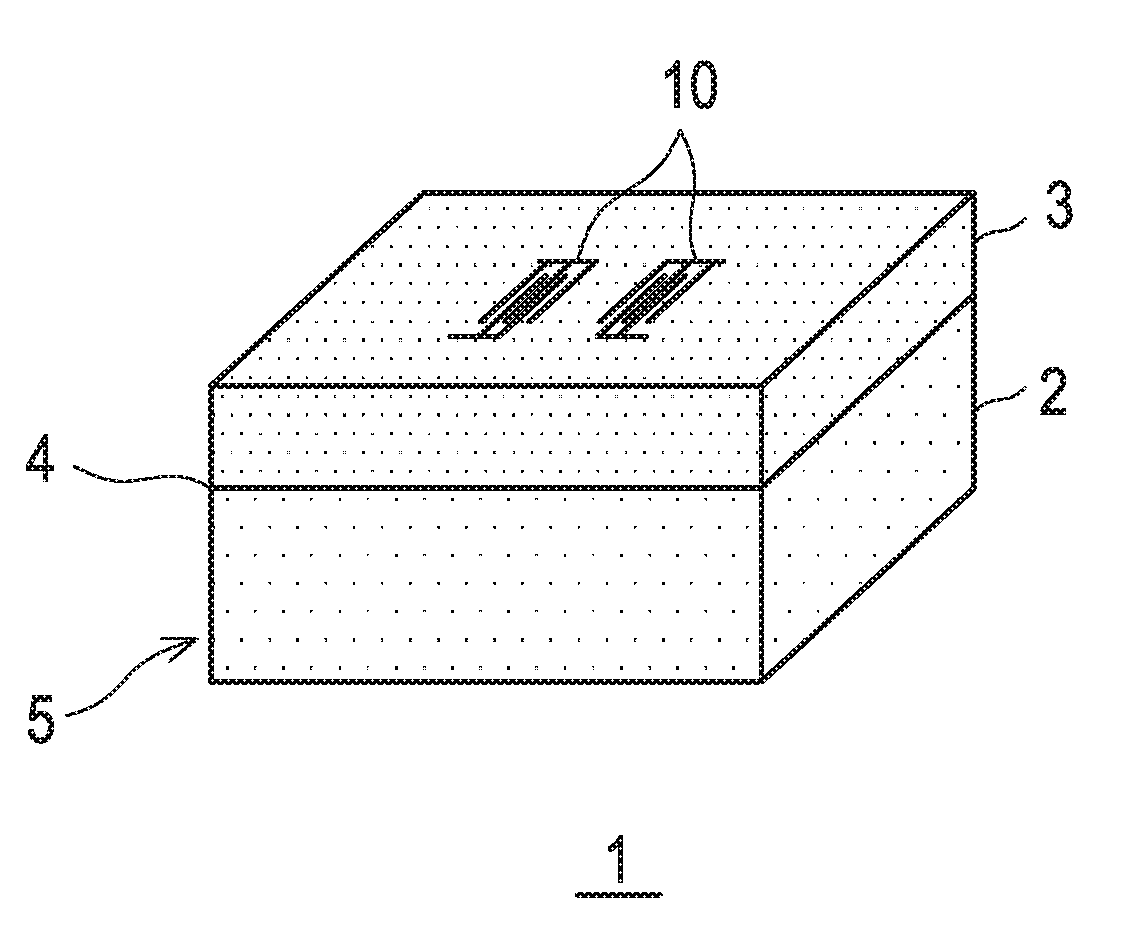
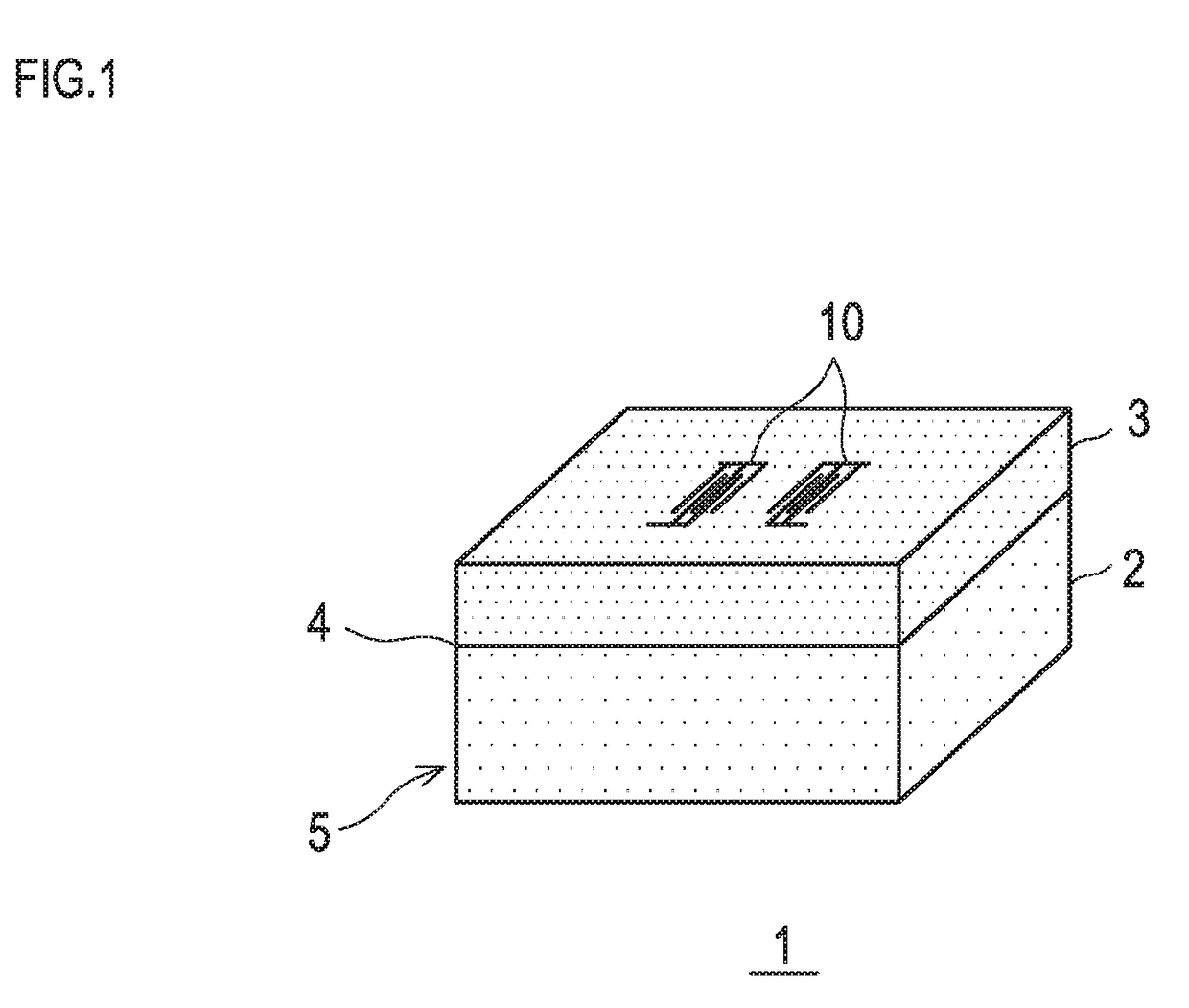
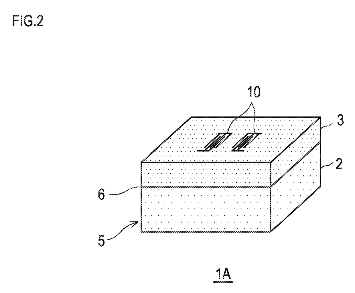
[0091]A bonded substrate was obtained based on the aforementioned embodiment. A SAW resonator was provided on the principal surface of the piezoelectric substrate such that the propagation direction of an LLSAW was the X-direction.

[0092]In this example, as the piezoelectric substrate, lithium tantalate was used in which the thickness was 100 μm and the plane orientation was X-cut and 31° Y-propagating. Moreover, as the quartz substrate, a crystal that was grown by a hydrothermal synthesis method and cut out in the ST-cut direction to have 250 μm of thickness was used.

[0093]The bonded sample was polished on the lithium tantalate side to be thin with approximately 10 μm of thickness.

[0094]For the sample material obtained by making the piezoelectric substrate thin after bonding the quartz substrate and the piezoelectric substrate, a phase velocity and an electromechanical coupling factor of an LLSAW were calculated, the ...


PUM

PropertyMeasurementUnit
Thicknessaaaaaaaaaa
Thicknessaaaaaaaaaa
Angleaaaaaaaaaa

Abstract

There is provided a bonded substrate including: a quartz substrate; and a piezoelectric substrate which is bonded on the quartz substrate and on which a surface acoustic wave propagates, wherein the quartz substrate and the piezoelectric substrate are bonded at a bonding interface through covalent bonding, and a surface acoustic wave element having a higher phase velocity and a higher electromechanical coupling factor than conventional one is obtained by disposing an interdigital electrode on a principal surface of the piezoelectric substrate.

Description

[0001]The present U.S. patent application claims a priority under the Paris Convention of Japanese patent application No. 2016-157122 filed on Aug. 10, 2016, the entirety of which is incorporated herein by references.BACKGROUND OF THE INVENTIONField of the Invention[0002]The present invention relates to a bonded substrate using a surface acoustic wave, a surface acoustic wave element, a surface acoustic wave device, and a method of manufacturing the bonded substrate.Description of the Related Art[0003]With progress of mobile communication devices such as a mobile phone, high-performance surface acoustic wave (surface acoustic wave: SAW) devices are being also requested. In particular, for high-frequency and broadband operation, SAW substrates are being requested to have a high-speed and high-coupling SAW mode, and excellent temperature characteristics for preventing a passband from moving due to temperature change.[0004]Furthermore, a longitudinal-type leaky surface acoustic wave (a...

Claims


Application Information

Patent Timeline
IPC IPC(8): H03H9/02H03H9/64H03H3/08H03H9/25
CPCH03H9/02551H03H9/25H03H9/02559H03H9/64H03H3/08H03H9/02574H03H9/145Y10T29/42H10N30/072
Inventor KURIMOTO, KOUHEIKISHIDA, KAZUHITOKAYANO, RINZOMIZUNO, JUNKAKIO, SHOJI
Owner JAPAN STEEL WORKS LTD
Why Eureka
Try Eureka