Anti-reflective and Anti-fogging materials
- Summary
- Abstract
- Description
- Claims
- Application Information
AI Technical Summary
Benefits of technology
Problems solved by technology
Method used
Image

Examples
example 1
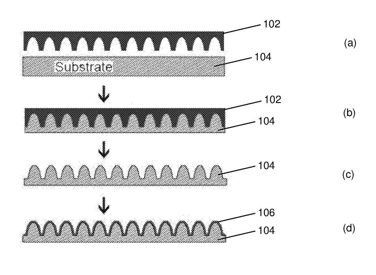
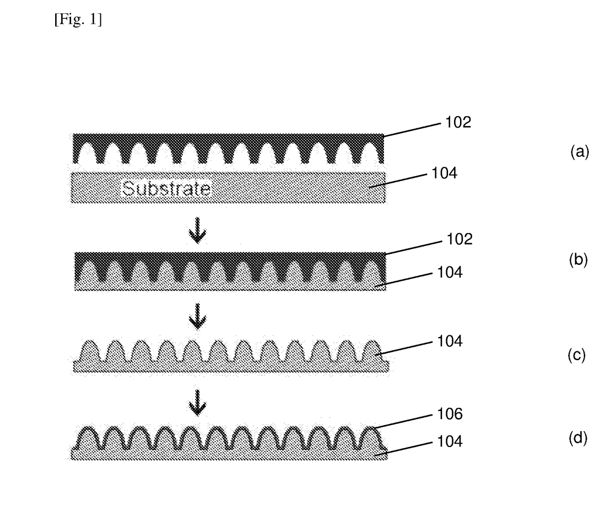
[0054]A schematic diagram illustrating a process to prepare a textured polymer substrate in accordance with an embodiment of the present disclosure is shown in FIG. 1.
[0055]In step (a) of FIG. 1, 102 is used as a mold to imprint a surface of a substrate 104. Mold 102 has nano-sized surface features complementary to the nano-sized surface features desired to be formed onto the surface of substrate 104. The nano-sized surface features may be of a size smaller than the wavelength of light, thereby creating a graded refractive index to increase the transmission of light. The surface of substrate 104 may be a plain, unpatterned surface of substrate 104 or the surface of micro-sized features integrally formed on substrate 104. Where the surface of substrate 104 is a surface of micro-sized features integrally formed on substrate 104, an optional step prior to step (a) comprises forming micro-sized features on substrate 104. Step (b) is performed at conditions to create imprints on the surf...
example 1a
[0057]In Example 1a, the optional step prior to step (a) is demonstrated by using a nanoimprint lithography technique. Nanoimprint lithography is a simple, low cost, high throughput and high resolution surface patterning technique. An advantage of nanoimprint lithography is that the resolution of the resulting nanoimprints can be as small as 5 nm.
[0058]A nickel metal mold with specific micro-sized features was pressed onto a polycarbonate (PC) film of 250 μm in thickness and an area of 2 cm×2 cm. Polycarbonate substrates are commonly used as plastic material for equipment such as goggles, eyewear and visors.
[0059]The micro-sized features of the mold were complementary to the micro-sized surface features desired to be formed onto the substrate. The micro-sized surface features desired on the substrate may be geometrically selected to be biomimetic, such as ommatidia-like structures. In this example, the micro-sized surface features desired on the substrate were hexagonally arrayed le...
example 1b
[0062]In Example 1b, steps (a), (b) and (c) of FIG. 1 are demonstrated, also by using nanoimprint lithography.
[0063]A nickel metal mold with specific nanostructures was pressed onto a surface of a polycarbonate (PC) film of 250 μm in thickness and an area of 2 cm×2 cm to imprint the PC film. The nano-sized features of the mold were complementary to the nano-sized surface features desired to be formed onto the surface of the substrate. The nano-sized surface features desired on the substrate may be nano-cones.
[0064]The temperature for the imprinting step was chosen to be a temperature below the glass transition temperature of polycarbonate to enable the formation of nano-sized surface features integrally on the micro-sized features of the imprinted film of Example 1a. Specifically, the imprinting was conducted at 150° C. and 50 bars.
[0065]Thereafter, the imprinted film was cooled down to 50° C. and the pressure was released. The imprinted film was then cooled down to room temperature...
PUM
| Property | Measurement | Unit |
|---|---|---|
| Thickness | aaaaa | aaaaa |
| Diameter | aaaaa | aaaaa |
| Nanoscale particle size | aaaaa | aaaaa |
Abstract
Description
Claims
Application Information
 - Generate Ideas
- Intellectual Property
- Life Sciences
- Materials
- Tech Scout
- Unparalleled Data Quality
- Higher Quality Content
- 60% Fewer Hallucinations
Browse by: Latest US Patents, China's latest patents, Technical Efficacy Thesaurus, Application Domain, Technology Topic, Popular Technical Reports.
© 2025 PatSnap. All rights reserved.Legal|Privacy policy|Modern Slavery Act Transparency Statement|Sitemap|About US| Contact US: help@patsnap.com