CVD reactor and method for nanometric delta doping of diamond

a reactor and delta doping technology, applied in the direction of electrical equipment, semiconductor/solid-state device testing/measurement, electric discharge tubes, etc., can solve the problems of insufficient thermal activation energy barrier, inability to demonstrate the theoretically expected performance of delta doping of diamond with boron, and relatively low concentration of free carriers, so as to minimize turbulence and gas mixing, the effect of constant loads or “impedances”

Active Publication Date: 2018-03-08
EUCLID TECHLABS LLC
View PDF5 Cites 2 Cited by
  • Summary
  • Abstract
  • Description
  • Claims
  • Application Information

AI Technical Summary

Benefits of technology

[0009]An apparatus and method is disclosed for creating nanometric delta doped layers in epitaxial diamond with interfaces between the doped and high mobility layers that are sufficiently abrupt and smooth to provide at least 100 cm2 / Vsec carrier mobility and 1013 cm−2 sheet carrier concentrations. The disclosed apparatus includes a novel switched-chamber gas supply that enables rapid switching between gas sources by maintaining constant loads or “impedances” on the outlets of the gas sources, thereby minimizing any turbulence and gas mixing caused by the switching. The method further includes preparation of an atomically smooth, undamaged single crystal diamond substrate surface by finely polishing the surface, preferably in or near the (100) plane, and then etching the surface after polishing to remove any subsurface polishing damage. Embodiments of the method further include maintaining rapid gas flows while adopting extraordinarily slow growth rates to create the sharpest possible interfaces.

Problems solved by technology

However, a major barrier to exploiting diamond for active electronic applications is that there are no dopants known that have a sufficiently low thermal activation energy barrier to create a concentration of electronic carriers and a carrier mobility in diamond at room temperature that is adequate for most devices of interest.
However, this activation energy is still high enough to ensure that only a fraction of the boron present is activated at room temperature, leading to relatively low concentrations of free carriers.
Unfortunately, as the activation energy of the holes decreases, so does carrier mobility, not only because of the increased impurity scattering but also due to the onset of a low-mobility, hopping-like conduction.
Recent attempts at delta doping of diamond with boron have failed to demonstrate the theoretically expected performance, and have shown low carrier mobilities, low sheet carrier concentrations, and / or low channel mobility.
Some of these studies have attributed this disappointing performance to poor lateral homogeneity and interrupted morphology of the delta layers.

Method used


Image

  • CVD reactor and method for nanometric delta doping of diamond
  • CVD reactor and method for nanometric delta doping of diamond
  • CVD reactor and method for nanometric delta doping of diamond

Examples


Embodiment Construction

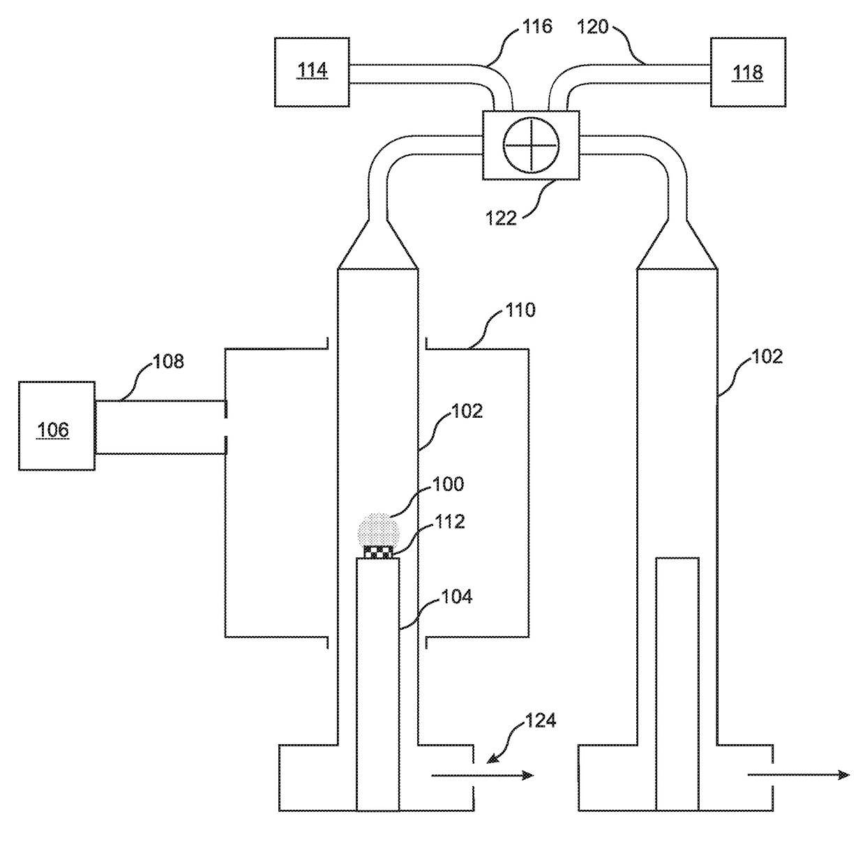
[0043]The present invention is an apparatus and method for creating nanometric delta doped layers in epitaxial diamond with interfaces between the doped and high mobility layers that are sufficiently abrupt and smooth to provide at least 100 cm2 / Vsec carrier mobility and 1013 cm−2 carrier concentration.

[0044]The apparatus of the present invention is a CVD reactor that is able to create nanometric delta-doped layers with ultra-sharp interfaces between doped / undoped material. FIG. 1 is a schematic illustration of an embodiment of the disclosed reactor, in which a microwave plasma excitation zone 100 surrounds a substrate 112 supported by a substrate holder 104 in a reduced pressure region of a vertical quartz tube growth chamber 102. In various embodiments the growth chamber is a fused silica tube 102. In embodiments, the substrate holder 104 can heat the substrate 112 to a temperature of between 700 and 1100° C. as desired.

[0045]The plasma in this embodiment is produced by electromag...


PUM

PropertyMeasurementUnit
temperatureaaaaaaaaaa
roughness Saaaaaaaaaaa

Abstract

An apparatus and method for creating nanometric delta doped layers in epitaxial diamond includes providing a dummy gas load with gas impedance equivalent to the reactor, and switching gas supplied between the reactor and the gas dummy load without stopping either flow, thereby enabling rapid flow and rapid gas switching without turbulence. An atomically smooth, undamaged substrate can be prepared, preferably in the (100) plane, by etching the surface after polishing to remove subsurface damage. A gas phase chemical getter reactant such as hydrogen disulfide can be used to suppress incorporation of residual boron into the intrinsic layers. Embodiments can produce interfaces between doped and mobile layers that provide at least 100 cm2/Vsec carrier mobility and 1013 cm−2 sheet carrier concentration.

Description

FIELD OF THE INVENTION[0001]The invention relates to reactors and methods for epitaxial growth of diamond, and more particularly to chemical vapor deposition (“CVD”) reactors and methods for creating nanometric delta doped layers in epitaxially grown single crystals of diamond.BACKGROUND OF THE INVENTION[0002]Diamond is of strong interest as a potential semiconductor material for high voltage, high frequency, and / or high power active and passive electronic devices because of its superlative materials properties, including high electronic carrier mobilities, high breakdown field strength, high thermal diffusivity, favorable matrix for quantum devices, as well as many other desirable optical, chemical, and materials properties. However, a major barrier to exploiting diamond for active electronic applications is that there are no dopants known that have a sufficiently low thermal activation energy barrier to create a concentration of electronic carriers and a carrier mobility in diamon...

Claims


Application Information

Patent Timeline
Patent Type & Authority Applications(United States)
IPC IPC(8): H01L21/02H01L21/66H01J37/32
CPCH01L21/02527H01L21/02024H01L21/02019H01L21/02376H01L21/0262H01L21/02584H01J2237/3321H01L21/02579H01L21/02634H01L21/02656H01J37/32449H01J37/32724H01J37/32201H01L22/26H01J37/32192H01J37/32467H01L22/12H01L21/02658
Inventor BUTLER, JAMES E
Owner EUCLID TECHLABS LLC
Why Eureka
Try Eureka