Fabricating unique chips using a charged particle multi-beamlet lithography system

a lithography system and multi-beamlet technology, applied in the field of manufacturing, can solve the problems of high production cost of masks used in this process, unsuitable for fabricating unique chips, and high cost of manufacturing unique chips for each single chip, so as to minimize the public exposure of selection data

Active Publication Date: 2018-05-03
ASML NETHERLANDS BV
View PDF11 Cites 6 Cited by
  • Summary
  • Abstract
  • Description
  • Claims
  • Application Information

AI Technical Summary

Benefits of technology

[0010]One way of making such electronic devices unique is by selecting different sets of features to be used for making different individual electronic devices of a set of electronic devices, thereby individualizing the electronic devices. Such a set of electronic devices may be devices which all perform the same function, such as providing a predetermined electronic output as a response to a certain predetermined electronic input. Such devices may be used, for example, in secure systems for providing a response enabling secure identification of the device. When the predetermined input is presented to the electronic devices during use, different outputs are generated by each individualized electronic device, thus enabling secure identification of the device.
[0012]It is also possible to create the individualized part of the electronic device and the common part of the electronic device separately. For example, the common design layout part may be created utilizing photolithography at a relatively lower cost, while the individualized part may be created using a maskless lithography system. The to be individualized part of the electronic device can be individualized by selecting different features for different subsets of the electronic devices. The selection of the features can be made at a late processing stage close to or within the maskless lithographic exposure system, thereby minimizing the potential for public exposure of the specific features used to individualize a particular electronic device.
[0017]Advantageously the method enables the creation of the individualized area of the electronic devices to remain within the operations of the maskless lithographic exposure system and public exposure time of the design data of the individualized area is minimized.
[0019]Advantageously the required processing power and memory for generating the beamlet control data may remain low, in that the design layout data can be reused for the creation of multiple electronic devices, where utilizing the known method of creating unique electronic devices requires design layout data for each unique electronic device and thus capacity and processing time for each unique design manufactured.
[0036]The beamlet control data may be encrypted to provide additional data security within the fab in the process of creating unique electronic devices.
[0041]The black box may be owned by a third party, e.g. an IP block owner or the owner of the manufactured chip, or a key management infrastructure owner. Advantageously the black box can be located within the fab close to the operations of the lithography machine, thereby minimizing public exposure of the selection data. This in contrast to known chip manufacturing solutions, where a black box for individualizing chips is typically located outside of the fab and used to individualize the chips after being created.

Problems solved by technology

The masks used in this process are expensive to produce, and manufacturing a unique mask for each single chip is clearly much too expensive, for which reason mask based photolithography is considered unsuitable for fabricating unique chips.
A straight forward method of creating secure, at least unique devices, i.e. using the known maskless exposure system, may however not be optimized, at least adapted for securely producing unique electronic devices.

Method used


Image

  • Fabricating  unique chips using a charged particle multi-beamlet lithography system
  • Fabricating  unique chips using a charged particle multi-beamlet lithography system
  • Fabricating  unique chips using a charged particle multi-beamlet lithography system

Examples


Embodiment Construction

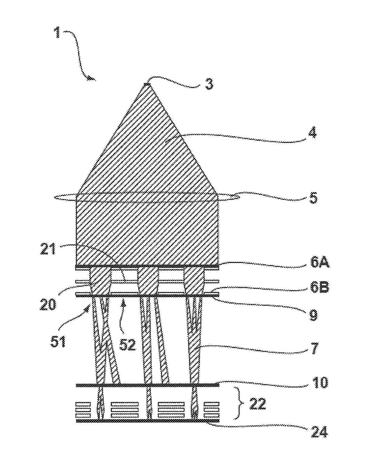
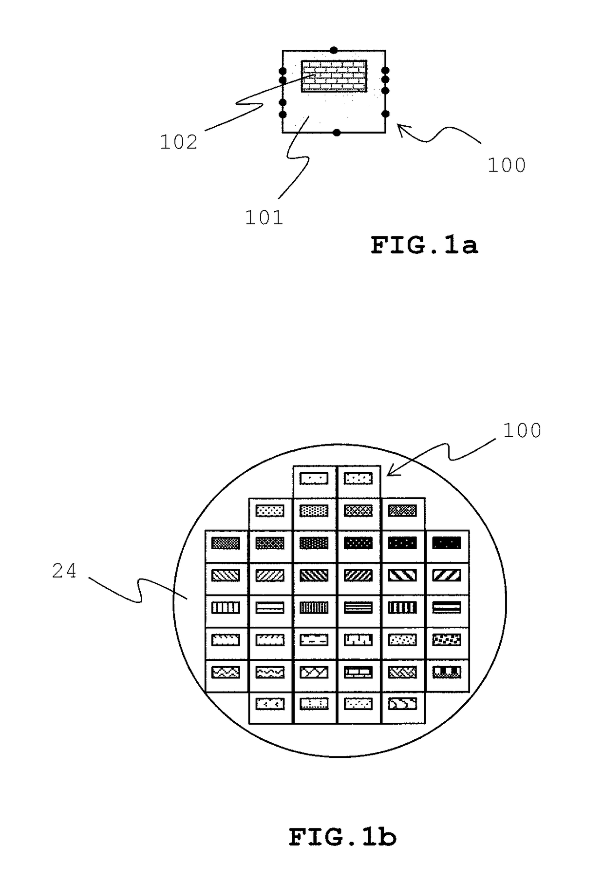
[0065]In the following examples reference is made to semi-conductor chips, but it is to be understood that the invention is not limited to chips and applies more generally to the creation of electronic devices having individualized, e.g. unique features. The electronic device may be a read only memory (ROM). For example, batches of chips with individualized ROM load may be created using the invention. Such batches are typically small batches, e.g. created from one or less than one wafer.

[0066]The process performed by charged particle multi-beamlet lithography is also being referred to as an electron beam or e-beam exposure. The electron beam exposure method is a maskless exposure method. The electron beams used for writing a target such as a wafer during electron beam exposure are also being referred to as beamlets.

[0067]Unique chips are designed to be unique with respect to other chips. This does not exclude the possibility that more than one unique chip can be made using the inven...


PUM

PropertyMeasurementUnit
acceleration voltageaaaaaaaaaa
diameteraaaaaaaaaa
widthaaaaaaaaaa

Abstract

Method of manufacturing electronic devices using a maskless lithographic exposure system using a maskless pattern writer. The method comprises generating beamlet control data for controlling the maskless pattern writer to expose a wafer for creation of the electronic devices, wherein the beamlet control data is generated based on a feature data set defining features selectable for individualizing the electronic devices, wherein exposure of the wafer according to the beamlet control data results in exposing a pattern having a different selection of the features from the feature data set for different subsets of the electronic devices.

Description

TECHNICAL FIELD[0001]The invention relates to a method of manufacturing, i.e. fabricating electronic devices such as semi-conductor chips. More specifically, the invention relates to the fabrication of unique chips using a charged particle multi-beamlet lithography machine, wherein the uniqueness of the chips is defined by features included in the chips. Consequently the invention equally relates to unique chips produced using this new method of manufacture, as well as to so called “fabs”, i.e. manufacturing facilities applying this novel method, and to maskless lithographic exposure system adapted for executing the improved method of manufacture.BACKGROUND ART[0002]In the semiconductor industry, lithography systems are used to create, i.e. fabricate such electronic devices, typically in the form of integrated circuits formed on silicon wafer, commonly referred to as semiconductor chips. Photolithography utilizes reusable optical masks to project an image of a pattern representing t...

Claims


Application Information

Patent Timeline
Patent Type & Authority Applications(United States)
IPC IPC(8): G03F7/20H01L21/263H01L29/06H01L23/528H01L27/02H01L25/065
CPCG03F7/2059H01L21/263H01L29/0692H01L27/0617H01L29/0684H01L27/0207H01L25/0655H01L23/528G03F7/2061H01L21/76816G06F30/39H01L21/768G06F30/394
Inventor VAN KERVINCK, MARCEL NICOLAAS JACOBUSKUIPER, VINCENT SYLVESTERWIELAND, MARCO JAN-JACO
Owner ASML NETHERLANDS BV
Why Eureka
Try Eureka