Process Method for Refining Photoconverter to Bond-Package LED and Refinement Equipment System

a technology of refining equipment and photoconverter, which is applied in the direction of basic electric elements, electrical equipment, semiconductor devices, etc., can solve the problems of high product cost cannot be reduced, low yield of leds packaged by using a photoconverter, and impede development, so as to achieve low light emission efficiency and low production efficiency. , the effect of low yield

Active Publication Date: 2018-07-12
JIANGSU CHERRITY OPTRONICS CO LTD
View PDF3 Cites 10 Cited by
  • Summary
  • Abstract
  • Description
  • Claims
  • Application Information

AI Technical Summary

Benefits of technology

[0017]First, the new process method of bond-packaging an LED using a refined photoconverter provided by the present invention is a novel process flow of LED bond-packaging by continuous rolling, which solves the problems of low light emission efficiency, low production efficiency, and a low yield of the LED bond-packaged by using existing conventional processes such as a casting process, a screen printing process, an upper and lower flat plate molding process, a single roller pressing process, and the like. The present invention can meet a requirement of bond-packaging the LED by using a semi-cured organic silicone resin photoconverter, and enhance the production efficiency and yield of LED packages in industrialized batch production.
[0018]Secondly, the semi-cured photoconversion sheet having a special-shaped light-emitting surface layer appearing a shape of a cambered surface, a hemispheric surface, or a planar surface is fabricated on the shaped microporous carrier sheet, and then the semi-cured photoconversion sheet is refined. In this way, possible residual pores, sags and crests, or other flaws produced during processing in the photoconversion sheet can be effectively eliminated, thus significantly improving brightness and color uniformity, and light emission uniformity and efficiency of finished LED package elements.
[0019]Thirdly, by using a rolling principle, the present invention organically integrates three procedures of shaping of the special-shaped microporous carrier sheet, refining of a photoconversion sheet, and forming of LED package elements by roll-bonding, such that a process of adding an extra bonding layer in the prior art is omitted, and the quality of bond-packaging of the special-shaped photoconversion sheet and the flip chip LEDs is improved. Moreover, it is convenient to equip an equipment system for a continuous process and to carry out intelligent control, so as to meet a production requirement of LED packages in industrialized batch production. In this way, the production efficiency of industrialized LED packaging in batches is remarkably improved.
[0020]Fourthly, the new process method and refining equipment system that are provided by the present invention are widely applicable to a packaging process of bonding an organic silicone resin photoconverter to flip chip LEDs of different power, thus completely meeting a requirement of refining the product production process during industrialized LED packaging in batches.

Problems solved by technology

However, during actual application, limited by many factors such as chip failure, package failure, thermal overstress failure, electrical overstress failure, and / or assembly failure, especially limited by the package failure, the LED prematurely encounters luminous decay or loss of luminous efficacy, thus hindering development of the LED to be a novel energy-saving light source.
These processes and matched packaging equipment cannot desirably solve flaws such as pores and unequal thickness of the photoconverter made of the organic silicone resin, thus causing a low yield of the LEDs packaged by using a photoconverter.
In addition, due to low production efficiency, the high product costs cannot be reduced.
However, there exist the following obvious defects: First, after the surface of the LED chip is coated with the photoconverter made of the organic silicone resin through a screen printing process, due to thermal overstress in a subsequent baking and curing procedure, pores still occur in part of the photoconverter coating and the coated surface of the LED chip, thus forming sags and crests.
Secondly, after the sealing mode or lens cover is filled with the silica gel and packaged together with the photoconverter-coated LED chip, due to thermal overstress in the subsequent procedure of baking and curing the whole structure, pores still occur in part of the silica gel layer on the sealing mold or lens cover, thus forming sags and crests.
Because the thermal overstress impact on the LED chip cannot be resolved in the packaging procedure, LED luminous efficacy is reduced inevitably.
Thirdly, an intelligent control system is not equipped to control the whole LED chip packaging process, which directly affects improvement of the yield.
However, there exist the following obvious defects: First, in a curing procedure of the fluorescent resin composition of the photoconverter, due to thermal overstress, pores still occur in part of the photoconverter surface layer, thus forming sags and crests.
Secondly, the LED coated with the photoconverter layer is still affected by the thermal overstress, causing a decrease in luminous efficacy of the LED in use.
Thirdly, the stages of the whole packaging process are complicated, causing low production efficiency of LED packages.
Fourthly, an upper and lower flat plate molding process may cause displacement of a flip chip, thus inevitably reducing the yield.
However, there exist the following obvious defects: First, the used fluorescent resin sheet is a cured fluorescent resin sheet, and therefore, possible residual pores, sags and crests, or other flaws produced during processing cannot be effectively eliminated.
Secondly, in a bonding stage, a pressure is exerted by a pressurizing tool from a side of the semiconductor light-emitting element, which may damage the semiconductor light-emitting element.
Thirdly, in the bonding stage using an adhesive in the fluorophor-containing resin layer, it is difficult to eliminate residuals from the semiconductor light-emitting element after bonding, and pores easily occur in the bonding procedure, thus reducing the yield; in addition, existence of the bonding layer reduces light emission efficiency of the LED element.
Fourthly, the substrate under the fluorescent resin sheet bonded to the light emitting surface of the semiconductor light-emitting element is not removed, which directly affects luminous efficacy of the semiconductor light-emitting element.
Fifthly, the multiple regions of the fluorophor-containing resin layer are arranged in the lengthwise direction repeatedly to form columns, but actually it is complex to arrange the multiple regions of the fluorophor-containing resin layer in such a manner, thus affecting the packaging efficiency of the whole element.
An error in arrangement positions of the multiple regions directly affects the precision of subsequent bonding with the light-emitting element.
If the multiple regions cannot be rendered uniform in size and thickness, a severe problem of product inconsistency may emerge.
To sum up, how to overcome the defects in the prior art has become one of major difficulties to be solved urgently in the technical field of LED packaging using a photoconverter at present.

Method used


Image

  • Process Method for Refining Photoconverter to Bond-Package LED and Refinement Equipment System
  • Process Method for Refining Photoconverter to Bond-Package LED and Refinement Equipment System
  • Process Method for Refining Photoconverter to Bond-Package LED and Refinement Equipment System

Examples


embodiment 1

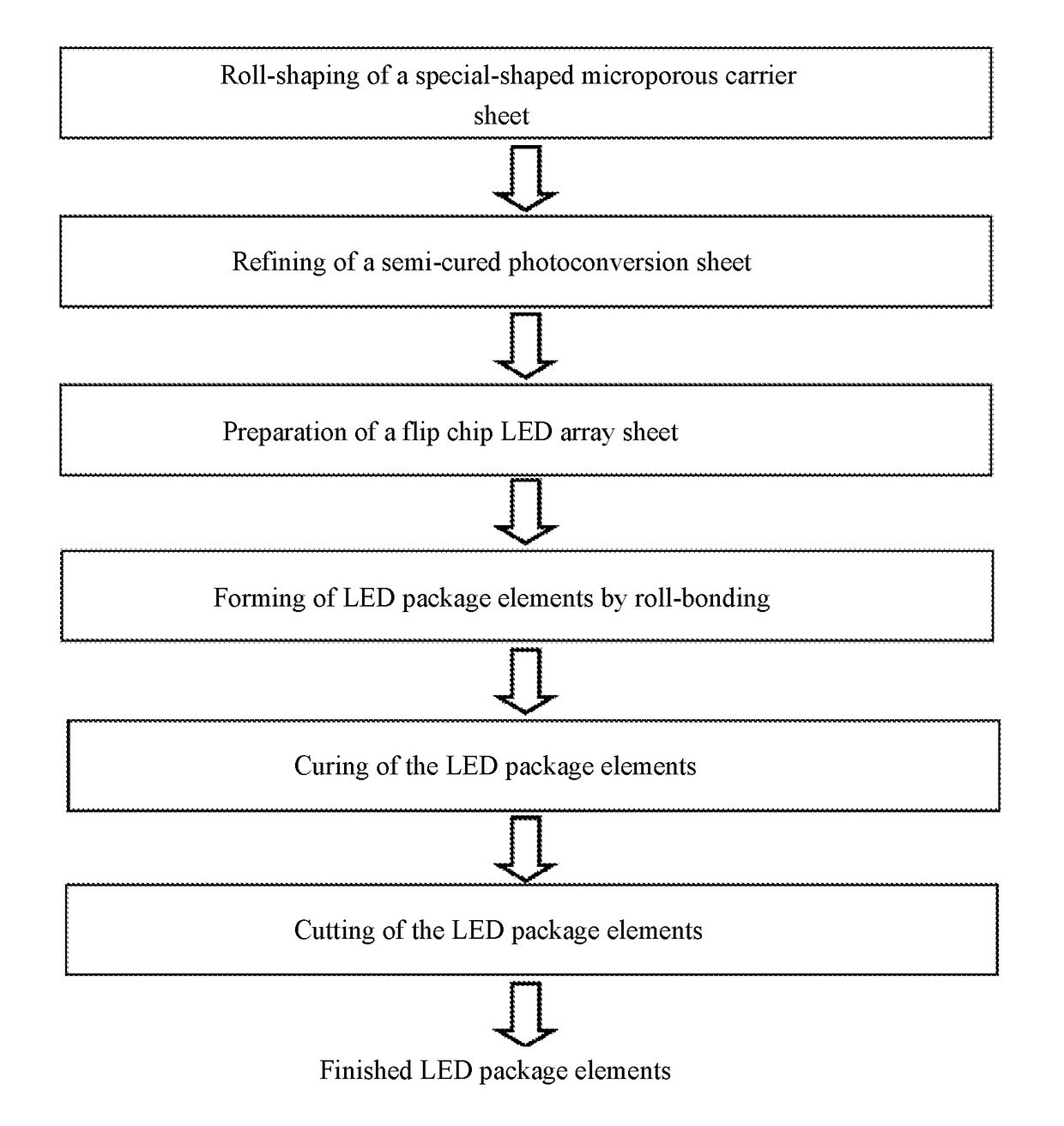
[0063]Referring to FIGS. 1, 2 and 6, a process method for bond-packaging an

[0064]LED using a refined photoconverter provided by the present invention includes the following continuous process flow: roll-shaping of a special-shaped microporous carrier sheet, refining of a semi-cured photoconversion sheet, preparation of a flip chip LED array sheet, forming of LED package elements by roll-bonding, curing of the LED package elements, and cutting of the LED package elements. The method specifically includes the following basic steps:

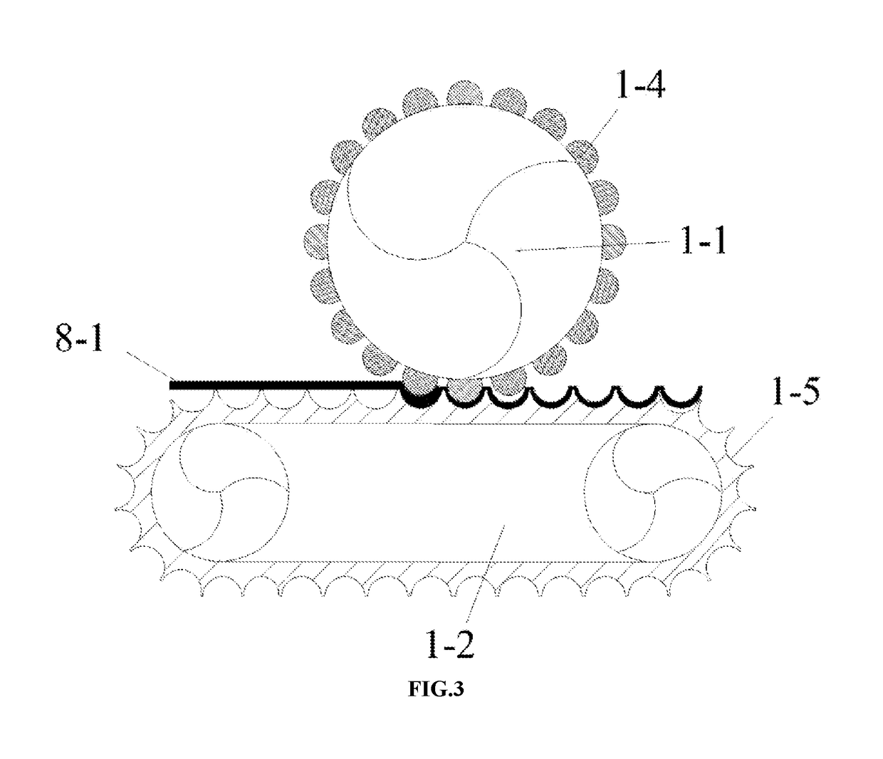
[0065]step 1: roll-shaping of a special-shaped microporous carrier sheet: performing roll-shaping on a microporous carrier sheet by using a first rolling device with a protrusion array and a second rolling device with a recess array that are disposed face-to-face and aligned with each other, to obtain a special-shaped microporous carrier sheet with a recess array, a micropore diameter of the microporous carrier sheet being not greater than 10 μm;

[0066]step 2...

embodiment 2

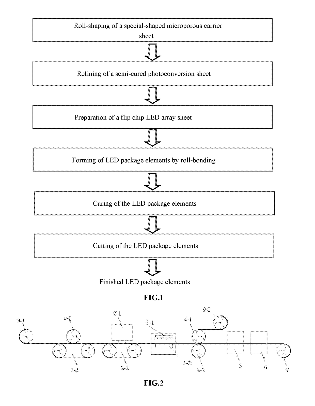
[0095]The present invention provides a refining equipment system applied to the process method for bond-packaging an LED using a refined photoconverter, which includes: a special-shaped microporous carrier sheet roll-shaping apparatus used for performing roll-shaping on a special-shaped microporous carrier sheet; a semi-cured photoconversion sheet refining apparatus used for forming a semi-cured photoconversion film on the shaped special-shaped microporous carrier sheet; and a roll-bonding apparatus used for forming LED package elements by roll-bonding, where the special-shaped microporous carrier sheet roll-shaping apparatus, the semi-cured photoconversion sheet refining apparatus, and the roll-bonding apparatus are sequentially arranged to form cooperatively linked process equipment.

[0096]The special-shaped microporous carrier sheet roll-shaping apparatus includes a first rolling device with a protrusion array and a second rolling device with a recess array that are disposed face-...


PUM

PropertyMeasurementUnit
diameteraaaaaaaaaa
temperatureaaaaaaaaaa

Abstract

Provided are a process method for bond-packaging an LED using a refined photoconverter, and a refining equipment system. The process method includes the following continuous process flow: roll-shaping of a special-shaped microporous carrier sheet, refining of a semi-cured photoconversion sheet, preparation of a flip chip LED array sheet, forming of LED package elements by roll-bonding, curing of the LED package elements, and cutting of the LED package elements. The present invention has a significant advantage of a refined photoconverter, and especially can meet a requirement of a continuous process flow of bond-packaging an LED using an organic silicone resin photoconverter, so as to enhance the production efficiency and yield of LED packages in industrialized batch production.

Description

TECHNICAL FIELD[0001]The present invention relates to the technical field of LED packaging using a photoconverter, and in particular, to a process method for bond-packaging an LED using a refined organic silicone resin photoconverter, and a refining equipment system.BACKGROUND[0002]With the advantages such as high brightness, low heat, long service life, and being environmentally friendly and renewable, LEDs are known as the most promising new generation of green light sources in the 21st century. At present, the theoretical service life of the LED can be over 100,000 hours. However, during actual application, limited by many factors such as chip failure, package failure, thermal overstress failure, electrical overstress failure, and / or assembly failure, especially limited by the package failure, the LED prematurely encounters luminous decay or loss of luminous efficacy, thus hindering development of the LED to be a novel energy-saving light source. To solve these problems, many sch...

Claims


Application Information

Patent Timeline
Patent Type & Authority Applications(United States)
IPC IPC(8): H01L33/50H01L33/52H01L33/00B29C59/04
CPCH01L33/50H01L33/52H01L33/005B29C59/04H01L2933/0041H01L33/44H01L33/04H01L33/501H01L33/62H01L2933/0033H01L33/48
Inventor HE, JINHUA
Owner JIANGSU CHERRITY OPTRONICS CO LTD
Why Eureka
Try Eureka