Display device

a display device and display technology, applied in the field of display devices, can solve the problems of distortion of a signal waveform delay in signal transmission to an end portion of a signal line, etc., and achieve the effects of deterioration of display quality, drop in voltage, and increase of wiring resistan

Active Publication Date: 2018-07-19
SEMICON ENERGY LAB CO LTD
View PDF6 Cites 18 Cited by
  • Summary
  • Abstract
  • Description
  • Claims
  • Application Information

AI Technical Summary

Benefits of technology

[0007]Increase in wiring resistance causes delay of signal transmission to an end portion of a signal line, distortion of a signal waveform, drop in voltage of a power supply line, or the like. As a result, deterioration of display quality, such as display unevenness or a defect in grayscale, increase in power consumption, or the like is caused. Furthermore, increase in the parasitic capacitance generated in a signal line also causes deterioration of display quality, increase in power consumption, or the like. For example, since the field-effect mobility of an amorphous silicon transistor is low, insufficient writing of an image signal due to increase in wiring resistance tends to occur easily in a display device including an amorphous silicon transistor.

Problems solved by technology

Increase in wiring resistance causes delay of signal transmission to an end portion of a signal line, distortion of a signal waveform, drop in voltage of a power supply line, or the like.
As a result, deterioration of display quality, such as display unevenness or a defect in grayscale, increase in power consumption, or the like is caused.
Furthermore, increase in the parasitic capacitance generated in a signal line also causes deterioration of display quality, increase in power consumption, or the like.
For example, since the field-effect mobility of an amorphous silicon transistor is low, insufficient writing of an image signal due to increase in wiring resistance tends to occur easily in a display device including an amorphous silicon transistor.

Method used


Image

  • Display device
  • Display device
  • Display device

Examples


embodiment 1

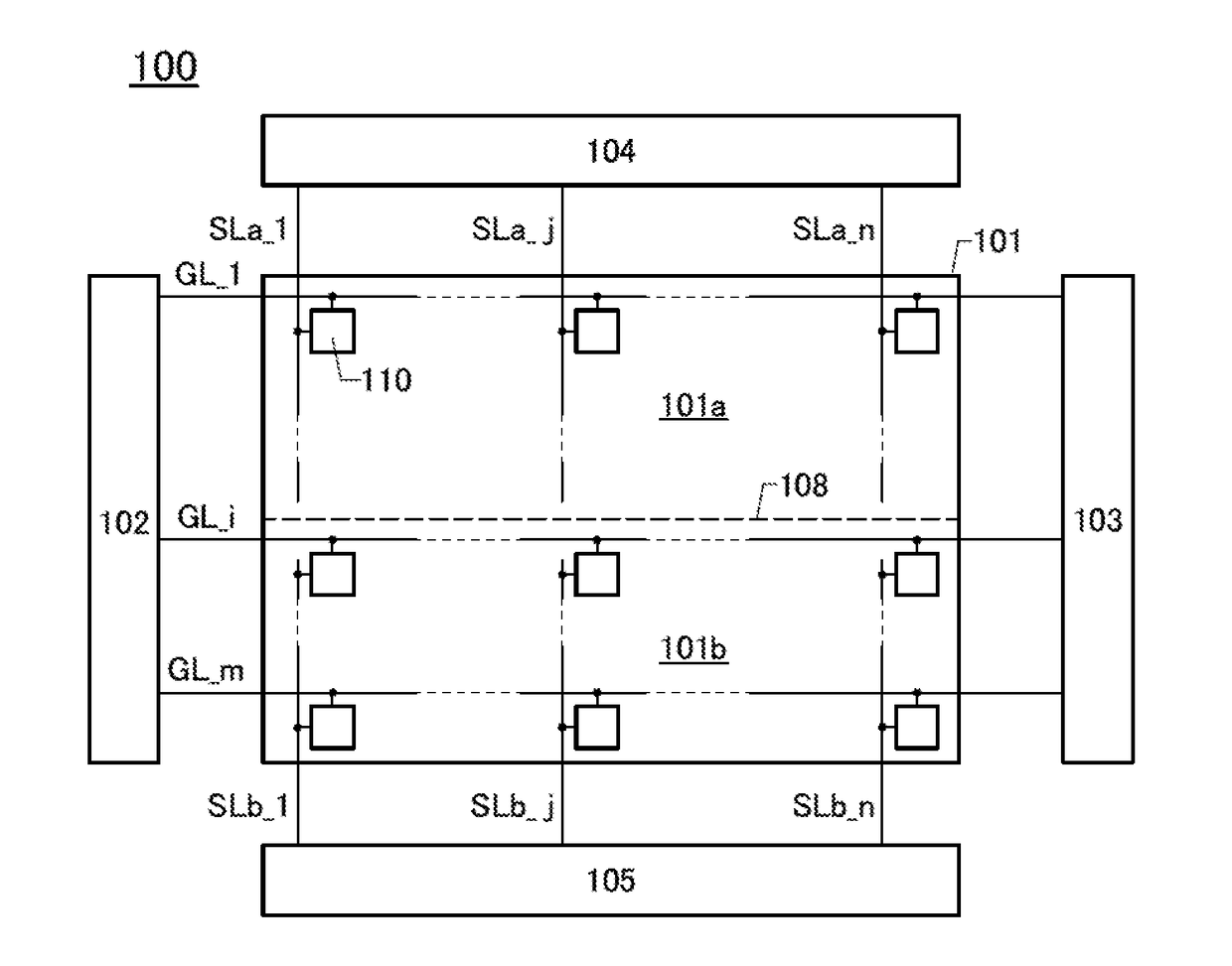
[0083]A display device 100 of one embodiment of the present invention will be described with reference to the drawings.

[0084]FIG. 1 is a block diagram of a configuration example of the display device 100. The display device 100 includes a display portion 101, a scan line driver circuit 102, a scan line driver circuit 103, a signal line driver circuit 104, and a signal line driver circuit 105. Note that circuits included in the scan line driver circuit 102, the scan line driver circuit 103, the signal line driver circuit 104, and the signal line driver circuit 105 are collectively referred to as a “peripheral driver circuit” or a “driver circuit” in some cases. Any of a variety of circuits such as a shift register, a level shifter, an inverter, a latch, an analog switch, and a logic circuit can be used as the peripheral driver circuit.

[0085]The display portion 101 includes a plurality of pixels 110. For example, the display portion 101 includes a plurality of pixels 110 arranged in a...

modification example 1

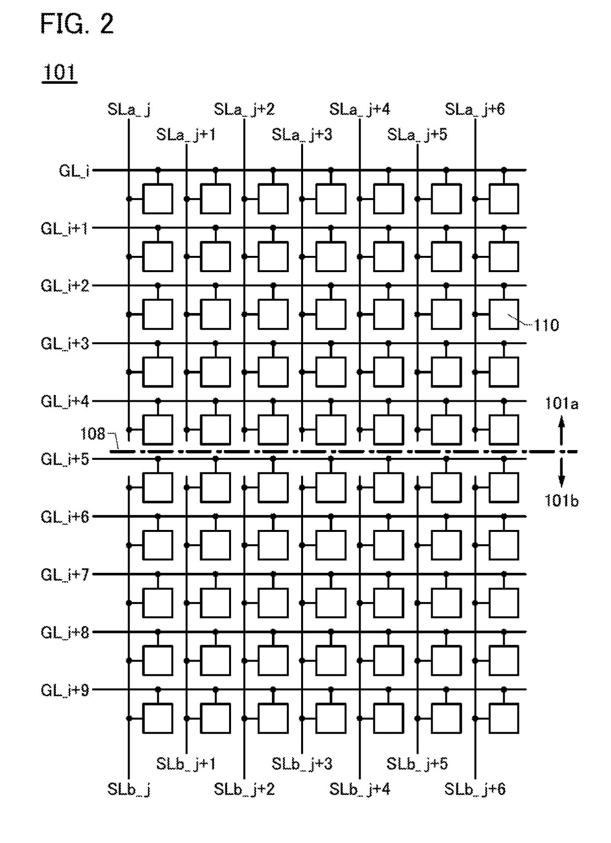
[0102]When the boundary line 108 is straight as shown in FIG. 2, a boundary portion between the display portion 101a and the display portion 101b is perceived as a stripe by a viewer of the display device in some cases. When the boundary line 108 is not straight as shown in FIG. 3, the display quality of the display device can be further improved.

[0103]For example, in the display portion 101, the lengths of the wiring SLa and the wiring SLb are varied randomly every column, whereby the boundary line 108 can be bent. Alternatively, in the display portion 101, the length of the wiring SLa in the j-th column (the wiring SLa_j) is made different from the length of the wiring SLa in the (j+1)-th column (the wiring SLa_j+1); similarly, in the display portion 101, the length of the wiring SLb in the j-th column (the wiring SLb_j) is made different from the length of the wiring SLb in the (j+1)-th column (the wiring SLb_j+1). Further alternatively, in the display portion 101, the ratio of t...

modification example 2

[0108]A double-source type display portion may be used as the display portion 101. FIG. 4 shows the display portion 101 that is a double-source type display portion in which the boundary line 108 is bent.

[0109]A double-source type display portion is a display portion in which two wirings SL are provided for pixels 110 in one column, and the pixel 110 electrically connected to one of the two wirings SL and the pixel 110 electrically connected to the other wiring SL are alternately arranged (see FIG. 4 and FIG. 5A). Furthermore, in the double-source type display portion, wirings GL in two rows can be selected at a time, so that the time of writing an image signal can be set long. Thus, insufficient writing of an image signal can be prevented even in high-speed driving at an increased frame frequency. For example, insufficient writing of an image signal can be prevented even at a frame frequency of higher than or equal to 120 Hz.

[0110]The frame frequency may be variable in the range fr...


PUM

PropertyMeasurementUnit
sizeaaaaaaaaaa
diagonal sizeaaaaaaaaaa
threshold voltageaaaaaaaaaa

Abstract

A display device with favorable display quality is provided. A display portion where a plurality of pixels is arranged in a matrix is divided into Region A and Region B, i.e., regions on the upstream side and the downstream side of a scanning direction. A signal line for supplying an image signal is provided in each of Region A and Region B. Region A and Region B adjoin each other such that a boundary line showing the boundary between the regions is bent. Bending the boundary line suppresses formation of a stripe in a boundary portion. For example, in a given column, the total number of pixels electrically connected to a signal line in Region A is made different from the total number of pixels electrically connected to a signal line in Region B.

Description

BACKGROUND OF THE INVENTION1. Field of the Invention[0001]One embodiment of the invention disclosed in this specification and the like relates to an object, a method, or a manufacturing method. One embodiment of the invention disclosed in this specification and the like relates to a process, a machine, manufacture, or a composition of matter. In particular, one embodiment of the invention disclosed in this specification and the like relates to a display device and a manufacturing method thereof.[0002]In this specification and the like, a semiconductor device generally means a device that can function by utilizing semiconductor characteristics. A display device (e.g., a liquid crystal display device and a light-emitting display device), a projection device, a lighting device, an electro-optical device, a power storage device, a memory device, a semiconductor circuit, an imaging device, an electronic device, and the like may be referred to as a semiconductor device. Alternatively, the...

Claims


Application Information

Patent Timeline
Patent Type & Authority Applications(United States)
IPC IPC(8): G09G3/36G02F1/1343G02F1/1362
CPCG09G3/3648G02F1/1343G02F1/136286G09G2310/0264G09G3/3233G09G2300/0426G09G2300/0452G09G2320/0223G02F1/1303G02F1/133602G02F1/13452G02F1/13458G06F1/1652H04M1/0268G02F2201/52H01L29/78648H01L27/124H01L27/1225G02B27/017G02F1/133391G02F1/13606G02B27/01
Inventor KOBAYASHI, HIDETOMOTAKAHASHI, KEIYAMAZAKI, SHUNPEI
Owner SEMICON ENERGY LAB CO LTD
Why Eureka
Try Eureka