Process Method Using Deformable Organic Silicone Resin Photoconverter to Bond-Package Led

a technology of organic silicone resin and photoconverter, which is applied in the direction of basic electric elements, electrical equipment, semiconductor devices, etc., can solve the problems of high product cost cannot be reduced, low yield of leds packaged by using a photoconverter, and impede development, so as to improve the production efficiency and yield of led packages

Active Publication Date: 2018-08-16
JIANGSU CHERRITY OPTRONICS CO LTD
View PDF3 Cites 1 Cited by
  • Summary
  • Abstract
  • Description
  • Claims
  • Application Information

AI Technical Summary

Benefits of technology

[0007]An objective of the present invention is to overcome the defects in the prior art and provide a process for bond-packaging an LED using a special-shaped organic silicone resin photoconverter. The present invention has a significant advantage of bond-pa

Problems solved by technology

However, during actual application, limited by many factors such as chip failure, package failure, thermal overstress failure, electrical overstress failure, and/or assembly failure, especially limited by the package failure, the LED prematurely encounters luminous decay or loss of luminous efficacy, thus hindering development of the LED to be a novel energy-saving light source.
These processes and matched packaging equipment cannot desirably solve flaws such as pores and unequal thickness of the photoconverter made of the organic silicone resin, thus causing a low yield of the LEDs packaged by using a photoconverter.
In addition, due to low production efficiency, the high product costs cannot be reduced.
However, there exist the following obvious defects: First, after the surface of the LED chip is coated with the photoconverter made of the organic silicone resin through a screen printing process, due to thermal overstress in a subsequent baking and curing procedure, pores still occur in part of the photoconverter coating and the coated surface of the LED chip, thus forming sags and crests.
Secondly, after the sealing mode or lens cover is filled with the silica gel and packaged together with the photoconverter-coated LED chip, due to thermal overstress in the subsequent procedure of baking and curing the whole structure, pores still occur in part of the silica gel layer on the sealing mold or lens cover, thus forming sags and crests.
Because the thermal overstress impact on the LED chip cannot be resolved in the packaging procedure, LED luminous efficacy is reduced inevitably.
Thirdly, no intelligent control system is equipped to control the whole LED chip packaging process, which directly affects improvement of the yield.
However, there exist the following obvious defects: First, in a curing procedure of the fluorescent resin composition of the photoconverter, due to thermal overstress, pores still occur in part of the photoconverter surface layer, thus forming sags and crests.
Secondly, the LED coated with the photoconverter layer is still affected by the thermal overstress, causing a decreas

Method used


Image

  • Process Method Using Deformable Organic Silicone Resin Photoconverter to Bond-Package Led
  • Process Method Using Deformable Organic Silicone Resin Photoconverter to Bond-Package Led
  • Process Method Using Deformable Organic Silicone Resin Photoconverter to Bond-Package Led

Examples


embodiment 1

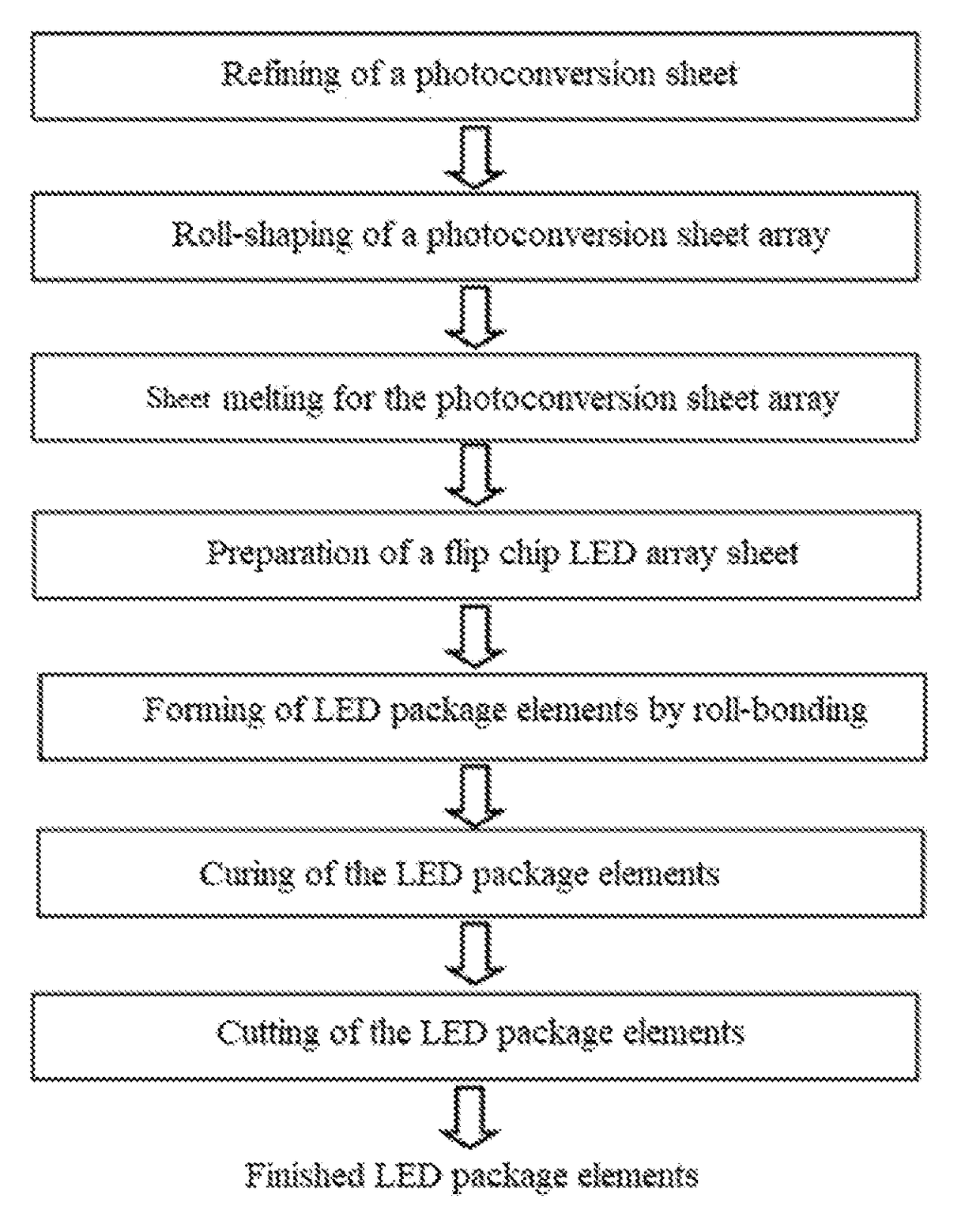
[0070] Referring to FIG. 1 and FIG. 2, the present invention provides a process for bond-packaging an LED using a special-shaped organic silicone resin photoconverter, which includes the following continuous process flow: roll-molding of a refined photoconversion sheet, roll-shaping of a photoconversion sheet array, sheet melting for the photoconversion sheet array, preparation of a flip chip LED array sheet, forming of LED package elements by roll-bonding, curing of the LED package elements, and cutting of the LED package elements. The process specifically includes the following steps:

[0071]step 1: roll-molding of a refined photoconversion sheet: in a vacuum heating condition, rolling a first outer protective film, a semi-cured photoconversion material, and a second outer protective film by using one or more sets of smooth-surface roll-laminating apparatuses, to obtain a refined photoconversion sheet formed by the first outer protective film, a semi-cured photoconversion sheet, and...

embodiment 2

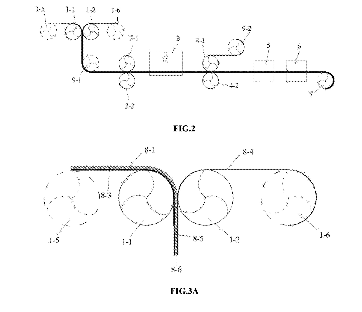
[0106] The present invention provides an equipment system applied to a process for bond-packaging an LED using a special-shaped organic silicone resin photoconverter, which includes: a smooth-surface roll-laminating apparatus used for refining a photoconversion sheet; a roll-shaping apparatus used for performing heating and roll-shaping on the refined photoconversion sheet; a sheet-melting apparatus used for performing sheet melting on the roll-shaped refined photoconversion sheet; and a roll-bonding apparatus used for performing roll-bonding on the sheet-melted refined photoconversion sheet and a flip chip LED array with a carrier film, the refined photoconversion sheet and the flip chip LED array facing each other and being aligned with each other. The roll-laminating apparatus, the roll-shaping apparatus, the sheet-melting apparatus, and the roll-bonding apparatus are arranged sequentially to form cooperatively linked process equipment. The roll-laminating apparatus includes one ...


PUM

PropertyMeasurementUnit
Temperatureaaaaaaaaaa

Abstract

A process method for bond-packaging an LED using a special-shaped organic silicone resin photoconverter includes the following continuous process flow: roll-molding of a refined photoconversion sheet, roll-shaping of a photoconversion sheet array, sheet melting for the photoconversion sheet array, preparation of a flip chip LED array sheet, forming of LED package elements by roll-bonding, curing of the LED package elements, and cutting of the LED package elements. The present invention has a significant advantage of bond-packaging an LED by continuous rolling, and can meet a condition requirement of bond-packaging an LED using a special-shaped organic silicone resin photoconverter, thereby enhancing the production efficiency and yield of LED packages in industrialized batch production.

Description

BACKGROUND OF THE INVENTIONField of the Invention[0001]The present invention relates to the technical field of LED packaging using a photoconverter, and in particular, to a process for bond-packaging an LED using a special-shaped organic silicone resin photoconverter.Description of Related Art[0002]With the advantages such as high brightness, low heat, long service life, and being environmentally friendly and renewable, LEDs are known as the most promising new generation of green light sources in the 21st century. At present, the theoretical service life of the LED can be over 100,000 hours. However, during actual application, limited by many factors such as chip failure, package failure, thermal overstress failure, electrical overstress failure, and / or assembly failure, especially limited by the package failure, the LED prematurely encounters luminous decay or loss of luminous efficacy, thus hindering development of the LED to be a novel energy-saving light source. To solve these p...

Claims


Application Information

Patent Timeline
IPC IPC(8): H01L33/54H01L33/56H01L33/26
CPCH01L33/54H01L33/56H01L33/26H01L2933/0033H01L33/005H01L33/505H01L2933/0041H01L2933/005H01L33/52H01L33/48H01L25/075B29C59/04H01L33/50
Inventor HE, JINHUA
Owner JIANGSU CHERRITY OPTRONICS CO LTD
Why Eureka
Try Eureka