Light-emitting element, light-emitting device, light source, authentication device, and electronic apparatus

a technology of light-emitting devices and light-emitting elements, applied in the field of light-emitting devices, light-emitting devices, light sources, authentication devices, and electronic devices, can solve the problems of increasing driving voltage and power consumption, and achieve the effect of excellent reliability

Inactive Publication Date: 2018-09-20
SEIKO EPSON CORP
View PDF17 Cites 2 Cited by
  • Summary
  • Abstract
  • Description
  • Claims
  • Application Information

AI Technical Summary

Benefits of technology

[0031]Such an electronic apparatus includes the light-emitting element in which the power consumption is suppressed, and therefore has excellent reliability.

Problems solved by technology

However, in such a light-emitting element, high efficiency and a long lifetime of the light-emitting element described above are achieved by using a tetracene-based host material as a host material of the light-emitting layer, however, a HOMO gap is present on a boundary surface between the light-emitting layer (host material) and the electron transport layer, and holes jump over the gap, and therefore, the light-emitting element has a problem that the driving voltage is increased, and also the power consumption is increased.

Method used


Image

  • Light-emitting element, light-emitting device, light source, authentication device, and electronic apparatus
  • Light-emitting element, light-emitting device, light source, authentication device, and electronic apparatus
  • Light-emitting element, light-emitting device, light source, authentication device, and electronic apparatus

Examples


example 1

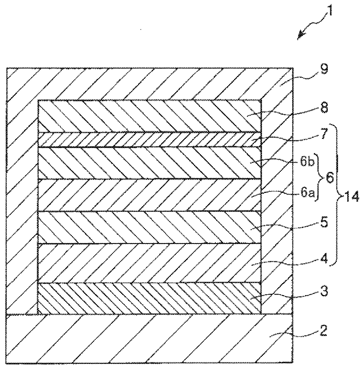
[0238] First, a transparent glass substrate having an average thickness of 0.5 mm was prepared. Subsequently, on this substrate, an ITO electrode (anode) having an average thickness of 100 nm was formed by a sputtering method.

[0239]Then, the substrate was subjected to ultrasonic cleaning while immersing the substrate in acetone and 2-propanol in this order, and thereafter subjected to an oxygen plasma treatment and an argon plasma treatment. Each of these plasma treatments was performed at a plasma power of 100 W and a gas flow rate of 20 sccm for a treatment time of 5 sec.

[0240] Subsequently, a compound represented by the above formula HIL-1 was deposited on the ITO electrode by a vacuum vapor deposition method, whereby a hole injection layer (HIL) having an average thickness of 70 nm was formed.

[0241] Subsequently, the constituent material of a light-emitting layer was deposited on the hole injection layer by a vacuum vapor deposition method, whereby a light-emitting layer having ...

example 2

[0248]A light-emitting element was produced in the same manner as in the above-mentioned Example 1 except that a compound represented by the above formula ETL2-3 was used as the compound used for forming the second electron transport layer in the step .

example 3

[0249]A light-emitting element was produced in the same manner as in the above-mentioned Example 1 except that a compound represented by the above formula (RD-1) was used as the light-emitting material (dopant) used in the step .


PUM


Abstract

A light-emitting element according to the invention includes an anode, a cathode, a light-emitting layer which is provided between the anode and the cathode, contains a light-emitting material and a first tetracene-based compound having a tetracene skeleton functioning as a host material that holds the light-emitting material, and emits light in a wavelength region of 600 nm or more by applying a current between the anode and the cathode, and an electron transport layer which is provided between the light-emitting layer and the cathode, and includes a first electron transport layer located on the cathode side and a second electron transport layer located on the light-emitting layer side and containing a second tetracene-based compound having a tetracene skeleton.

Description

BACKGROUND1. Technical Field[0001]The present invention relates to a light-emitting element, a light-emitting device, a light source, an authentication device, and an electronic apparatus.2. Related Art[0002]An organic electroluminescence element (so-called organic EL element) is a light-emitting element having a structure in which at least one layer of a luminous organic layer is interposed between an anode and a cathode. In such a light-emitting element, by applying an electric field between the cathode and the anode, an electron is injected into a light-emitting layer from the cathode side and also a hole is injected into the light-emitting layer from the anode side, and the electron and the hole are recombined in the light-emitting layer, whereby an exciton is generated, and energy generated when this exciton is returned to a ground state is released as light.[0003]As such a light-emitting element, there is known a light-emitting element which emits light in a long wavelength re...

Claims


Application Information

Patent Timeline
Patent Type & Authority Applications(United States)
IPC IPC(8): H01L51/50G06V10/143G06V10/147
CPCH01L51/5004H01L51/5012H01L51/5084H01L2251/552H01L2251/558H01L27/3244G06F1/1684H01L51/0054H01L51/0052H01L51/0072H01L51/0058G06K2009/0006G06K9/0012G06V40/1318G06V10/143G06V10/147H10K59/12H10K85/622H10K85/631H10K85/657H10K50/166H10K50/11G06V40/1341G06V40/1394H10K50/167H10K85/615H10K85/626H10K85/6572H10K2101/40H10K2101/30H10K2102/351
Inventor HAMADE, YUIGAFUJITA, TETSUJI
Owner SEIKO EPSON CORP
Why Eureka
Try Eureka