Double perovskite

a double perovskite and perovskite technology, applied in the field of double perovskite, can solve the problems of not being able to identify compounds matching the potential environmental impact of these devices, and the inability to match the remarkable optoelectronic properties of mapbi, etc., and achieve the effect of strong potential for optimizing lead-free perovskite photovoltaics

Active Publication Date: 2018-10-11
OXFORD UNIV INNOVATION LTD
View PDF4 Cites 15 Cited by
  • Summary
  • Abstract
  • Description
  • Claims
  • Application Information

AI Technical Summary

Benefits of technology

[0008]This new class of materials allows the use of lead (and other toxic heavy metals) to be avoided completely, providing a significant environmental benefit. The ma

Problems solved by technology

Despite the unprecedented progress in perovskite photovoltaics, the presence of lead in MAPbI3 raises concerns about the potential environmental impact of these devices.
However, to date no material can rival the remarkable optoelectronic properties of MAPbI3.
To check this possibility the inventors have performed a high-throughput computational screening of potential candidates

Method used


Image

  • Double perovskite
  • Double perovskite
  • Double perovskite

Examples


example 1

onal Study

Computational Setup

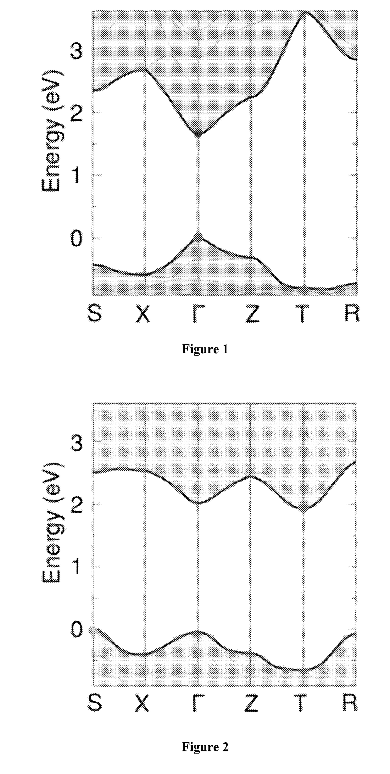
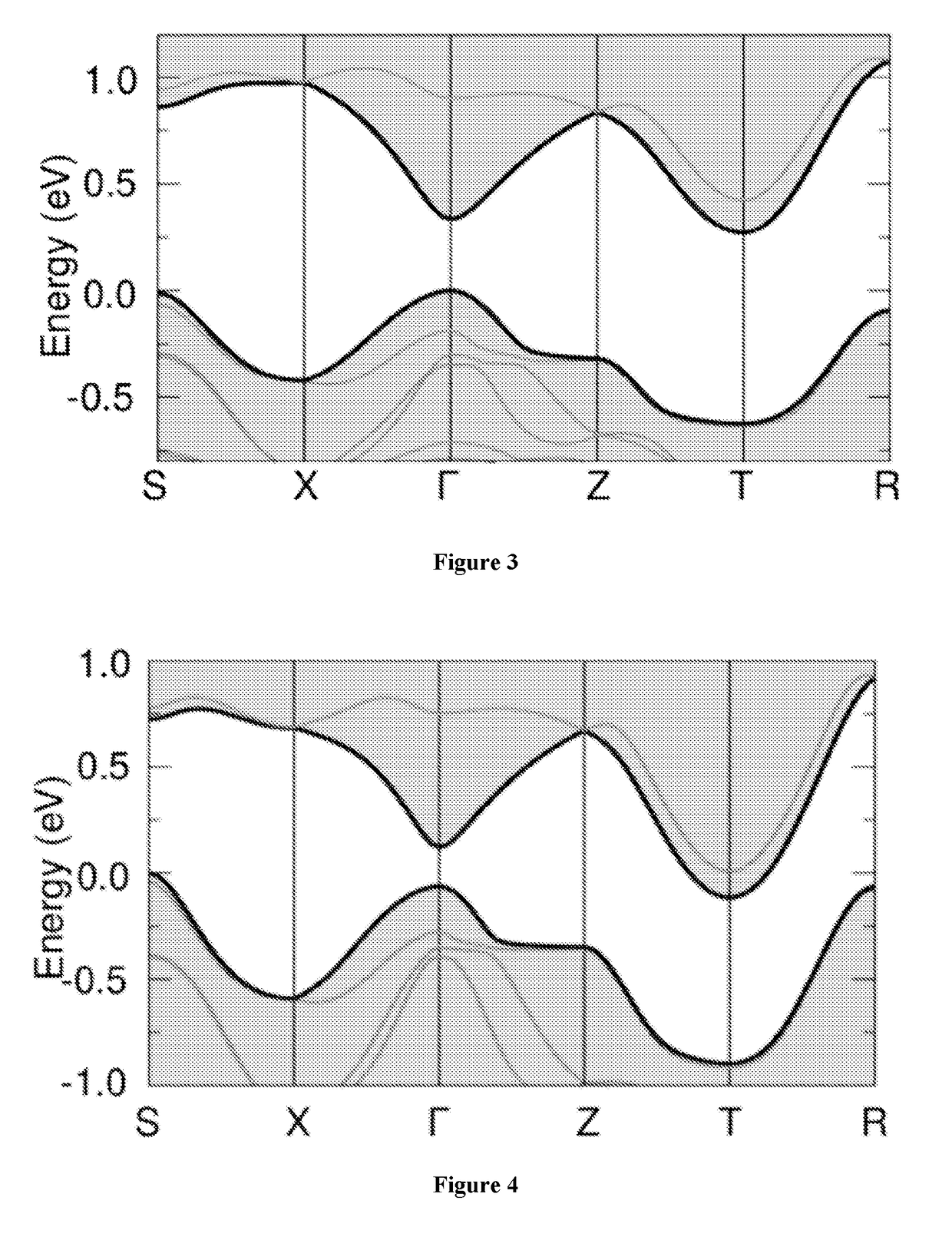
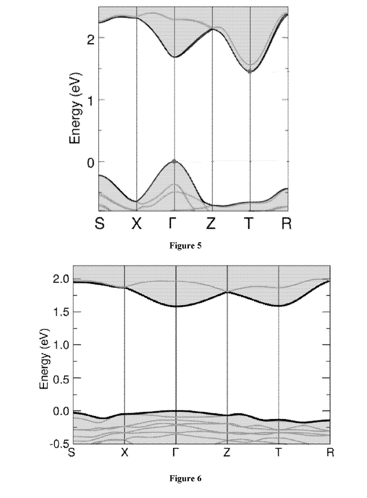
[0254]Structural optimisations were performed using DFT / LDA calculations, planewaves, and pseudopotentials, as implemented in the Quantum ESPRESSO distribution. For Cu, Ag, Au, and C, N, H, we use ultrasoft pseudopotentials including nonlinear core correction. For Bi and Sb we use norm-conserving pseudopotentials as in (Filip et al, quasiparticle band structures of stibnite, antimonselite, bismuthinite, and guanajuatite. Phys. Rev. B 87, 205125, 2013). All pseudopotentials are from the Quantum ESPRESSO library for reproducibility. The planewaves kinetic energy cutoffs for the wavefunctions and charge density are set to 60 / 70 Ry and 300 / 350 Ry for Bi / Sb perovskites, respectively. The Brillouin zone is sampled using an unshifted 6×6×6 grid. Forces and total energies are converged to 10 meV / A and 1 meV. All structural optimisations were carried out using scalar-relativistic LDA, while the band structures were from fully-relativistic calculations. The eigenv...

example 5

nescence Measurements

[0271]Measurements of the photoluminescence emission spectra of MA2AgBiI6 and FA2AgBiI6 were done using a Fluorolog spectrometer with excitation wavelength of 450 nm and measurements from 470 nm-800 nm with an integration time of 0.4 seconds. The results are shown in FIG. 12.

Example 6—Synthesis and Characterisation of Cs2BiAgCl6

[0272]Synthesis: Single-phase samples of Cs2BiAgCl6 were prepared by solid-state reaction in a sealed fused silica ampoule. For a typical reaction, the starting materials CsCl (Sigma Aldrich, 99.9%), BiCl3 (Sigma Aldrich, 99.99%) and AgCl (Sigma Aldrich, 99%) were mixed at a molar ratio of 2:1:1 respectively. The mixture was loaded in a fused silica ampoule that was flame sealed under vacuum (10−3 Torr). The mixture was heated to 500° C. over 5 hours and held at 500° C. for 4 hours. After cooling to room temperature, a yellow polycrystalline material was formed. Octahedral shaped crystals of length ˜0.1 mm could be extracted from the pow...


PUM


Abstract

The present invention relates to a semiconductor device comprising a semiconducting material, wherein the semiconducting material comprises a compound comprising: (i) one or more first monocations [A]; (ii) one or more second monocations [BI]; (iii) one or more trications [BIII]; and (iv) one or more halide anions [X]. The invention also relates to a process for producing a semiconductor device comprising said semiconducting material. Also described is a compound comprising: (i) one or more first monocations [A]; (ii) one or more second monocations [BI] selected from Cu+, Ag+ and Au+; (iii) one or more trications [BIII]; and (iv) one or more halide anions [X].

Description

FIELD OF THE INVENTION[0001]The present invention relates a semiconductor device comprising a semiconducting material and a process for producing a semiconductor device. The invention also relates to novel compounds comprising metal monocations.[0002]The work leading to this invention has received funding from the European Community's Seventh Framework Programme (FP7 / 2007-2013) under grant agreement agreements 279881, 239578 (ALIGN), 604032 of the MESO project and 604391 (Graphene Flagship).BACKGROUND OF THE INVENTION[0003]The development of efficient, cost-effective, and scalable solar energy technologies constitutes a top priority in the global energy research agenda. The past five years have witnessed a revolution in photovoltaics research with the discovery of the organic-inorganic perovskite methylammonium lead triiodide (MAPbI3, MA=CH3NH3), leading to solar cells with an energy conversion efficiency exceeding 20% (Green et al, The emergence of perovskite solar cells, Nature Ph...

Claims


Application Information

Patent Timeline
IPC IPC(8): C01G29/00H01L51/00H01L51/42H01G9/00H01G9/20
CPCC01G29/006H01L51/0091H01L51/009H01L51/0007H01L51/0028H01L51/4253H01G9/0036H01G9/2009H01G9/2018C01P2002/34C01P2002/72C01P2002/84C01P2002/77C01G30/006C01P2002/76Y02E10/549Y02E10/542H10K85/00H10K30/151H10K85/50H10K30/30H10K71/15H10K71/441H10K85/361H10K85/371
Inventor SNAITH, HENRY JAMESHAGIGHIRAD, AMIR ABBASGIUSTINO, FELICIANOFILIP, MARINAVOLONAKIS, GEORGE
Owner OXFORD UNIV INNOVATION LTD
Why Eureka
Try Eureka