Method of depositing film by peald using negative bias

Active Publication Date: 2019-01-31
ASM IP HLDG BV
View PDF3 Cites 224 Cited by
  • Summary
  • Abstract
  • Description
  • Claims
  • Application Information

AI Technical Summary

Benefits of technology

[0006]Some embodiments provide a method of forming a film on a substrate by plasma-enhanced atomic layer deposition (PEALD) in a reaction space defined by capacitively coupled first and second electrodes facing each other wherein the substrate is placed on the first electrode facing the second electrode, which PEALD comprises deposition cycles, each cycle comprising: (i) feeding a precursor in a pulse to the reaction space to adsorb the precursor on a surface of the substrate; (ii) after step (i), applying RF power to the second electrode to generate in the reaction space a plasma to which the precursor-adsorbed surface is exposed, thereby forming a sublayer on the surface; and (iii) applying a bias voltage to the second electrode while applying RF power in step (ii), said bias voltage being negative with reference to a potential on a surface of the first electrode, wherein the cycle is repeated to deposit multiple sublayers until a film constitut

Problems solved by technology

However, conventional PEALD using a capacitively coupled plasma (CCP) has the following problems.
However, strong ion bombardment exerted on a substrate surface causes problems.
However, when plasma

Method used


Image

  • Method of depositing film by peald using negative bias
  • Method of depositing film by peald using negative bias
  • Method of depositing film by peald using negative bias

Examples


example 1

Prophetic

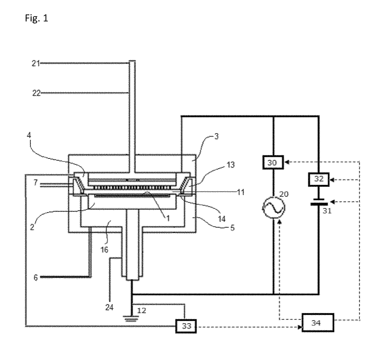
[0048]On a Si substrate (having a diameter of 300 mm and a thickness of 0.7 mm) having an organic film (polyimide film), a SiOCN film having a thickness of about 30 nm is deposited by PEALD using the apparatus illustrated in FIGS. 1, 3, and 4 using the sequence illustrated in FIG. 8, under conditions using an aminosilane ((3-aminopropyl)trimethoxysilane, APTMS) as a precursor, H2 as a reactant (H2 plasma), and Ar as a carrier gas, wherein the temperature of a bottle for the precursor is set at room temperature, the flow rate of H2 gas is about 100 sccm, and the flow rate of Ar gas is about 600 sccm, and the pressure is about 4 Torr, and the substrate temperature is about 200° C. RF power (a frequency of 13.56 MHz) applied to the upper electrode is about 200 W.

[0049]The bias voltage is applied to the upper electrode, using a voltage of 0 V, −50V, −100 V, −200 V, and −300 V, to overly the RF power in examples, respectively. After completion of the film deposition, the quality...

example 2

Prophetic

[0050]A SiOCN film having a thickness of about 30 nm is deposited on a polyimide film formed on a 300-mm Si wafer) using APTMS as a precursor, H2 as a reactant (H2 plasma), and Ar as a carrier gas, in a manner similar to that in Example 1, except that the bias voltage is changed as illustrated in FIG. 6. That is, in step “a”, the deposition cycle is repeated until the thickness of the SiOCN film reaches about 3 nm using the bias voltage determined in Example 1 where the degree of damage to the organic film is minimal, and then, in step “b”, the deposition cycle is continuously repeated until the thickness of the SiOCN film reaches about 5 nm (adding about 2 nm) using the bias voltage which is gradually increased in a negative direction (e.g., about −10 V / cycle) to the bias voltage determined in Example 1 where the quality of the SiOCN film is maximum (optimum), and then, in step “c”, the deposition cycle is continuously repeated until the thickness of the SiOCN film reaches...


PUM

PropertyMeasurementUnit
Thicknessaaaaaaaaaa
Electric potential / voltageaaaaaaaaaa
Frequencyaaaaaaaaaa

Abstract

A method of forming a film on a substrate by PEALD includes deposition cycles, each including (i) feeding a precursor in a pulse to a reaction space to adsorb a precursor on a surface of a substrate; (ii) after step (i), applying RF power to a second electrode to generate in the reaction space a plasma to which the precursor-adsorbed surface is exposed, thereby forming a sublayer on the surface; and (iii) applying a bias voltage to the second electrode while applying RF power in step (ii), which bias voltage is negative with reference to a potential on a surface of the first electrode, wherein the cycle is repeated to deposit multiple sublayers until a film constituted by the sublayers has a desired thickness.

Description

BACKGROUND OF THE INVENTIONField of the Invention[0001]The present invention generally relates to a method of forming a film on a substrate by plasma-enhanced atomic layer deposition (PEALD) using a capacitively coupled plasma (CCP) modified by a negative bias voltage.Description of the Related Art[0002]A dielectric film deposited by plasma-enhanced atomic layer deposition (PEALD) is widely used in the semiconductor manufacturing industry, since the conformality of such a film is very high, e.g., 100%, when being deposited in a trench having an aspect ratio of about 10. However, conventional PEALD using a capacitively coupled plasma (CCP) has the following problems. A plasma is an ionized gas containing positive ions and free electrons in proportions resulting in more or less no overall electric charge, and in PEALD using CCP, film formation is accomplished using ions and radicals. Ion bombardment is important to film growth and film quality. However, strong ion bombardment exerted ...

Claims


Application Information

Patent Timeline
IPC IPC(8): H01J37/32H01L21/02C23C16/455C23C16/44C23C16/505C23C16/40C23C16/34
CPCH01J37/32091H01L21/02274H01L21/0228C23C16/45536H01J2237/3321C23C16/505C23C16/401C23C16/34C23C16/4408C23C16/52H01L21/02126H01L21/02219H01L21/0337C23C16/36C23C16/45542C23C16/509H01L21/02205H01J37/32174
Inventor SUZUKI, TOSHIYA
Owner ASM IP HLDG BV
Why Eureka
Try Eureka