Interposer with a nanostructure energy storage device

a nanostructure energy storage and interposer technology, applied in the field of interposers, can solve the problems of reducing the physical area of defined components, high-speed integrated circuits are extremely sensitive to electrical noise, and the integration of such densely populated dies may come with a pri

Active Publication Date: 2019-02-14
SMOLTEK AB
View PDF0 Cites 2 Cited by
  • Summary
  • Abstract
  • Description
  • Claims
  • Application Information

AI Technical Summary

Benefits of technology

[0009]In view of the above-mentioned and other drawbacks of the prior art, it is an object of the present inv...

Problems solved by technology

Moreover, silicon dies can be stacked tier-to-tier on top of each other, which reduces the physical area for defined components.
However, integration of such densely populated dies may come with a price.
Many low-power, high speed integrated circuits are extremely sensitive to electrical noise generated by the continuous switching of the transistors located in the circuit blocks.
Such approaches however suffer from either the need for a substantial footprint of active silicon area, dielectric leakage, parasitic resistance, or are limited by the fundamental limitations in increasing in capacitance per unit area defined by the parallel plate...

Method used


Image

  • Interposer with a nanostructure energy storage device
  • Interposer with a nanostructure energy storage device
  • Interposer with a nanostructure energy storage device

Examples


Embodiment Construction

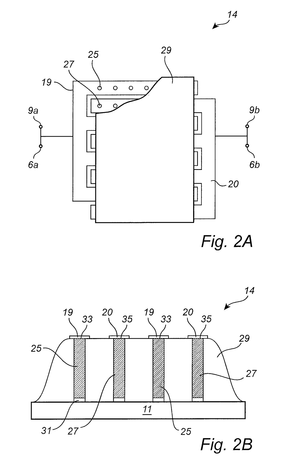
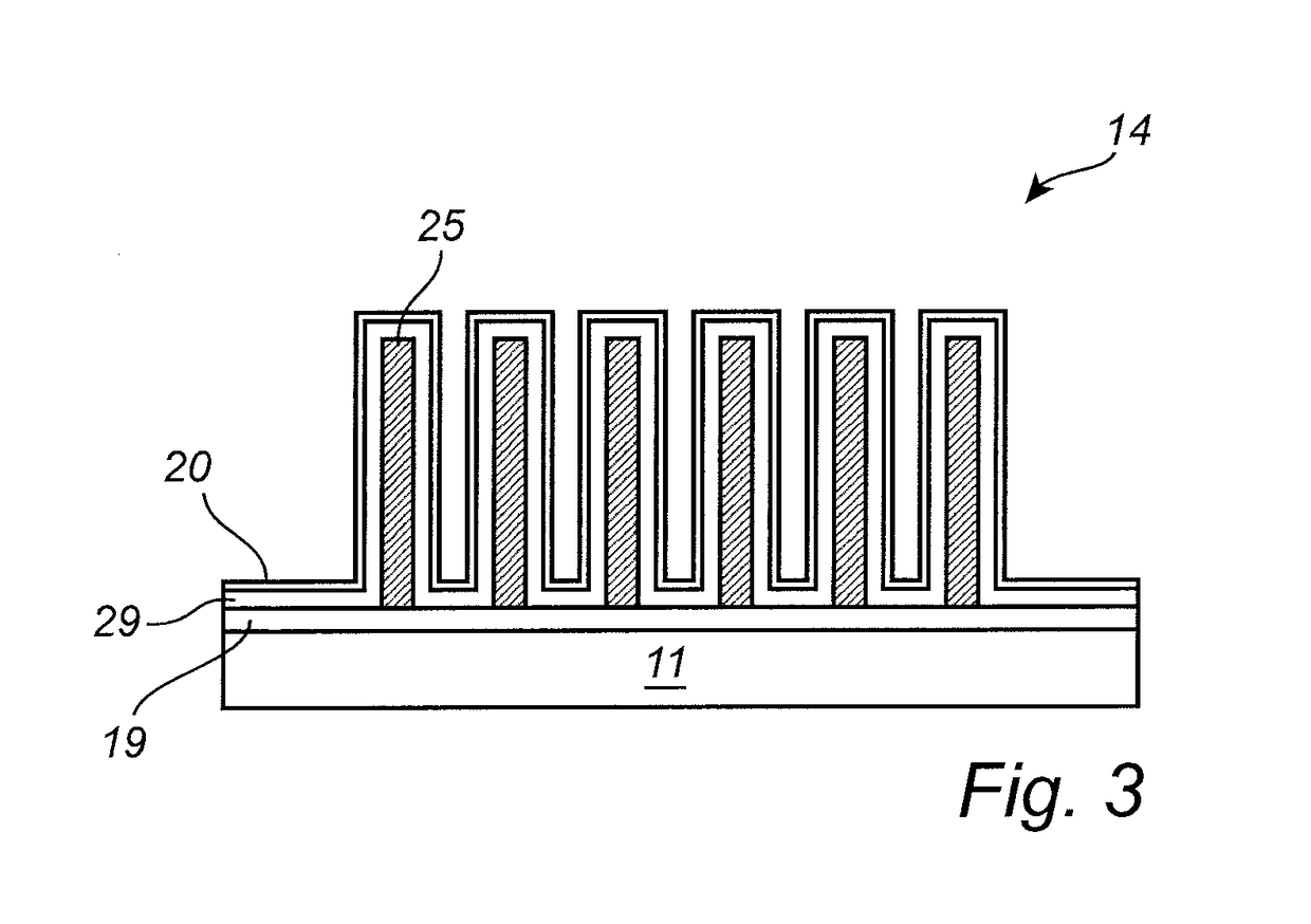
[0045]In the present detailed description, various embodiments of the energy storing interposer device is mainly described with reference to an energy storing interposer device comprising a nanostructure energy storage device in the form of a nanostructure capacitor.

[0046]It should be noted that this by no means limits the scope of the present invention, which equally well includes, for example, an interposer device comprising a nanostructure battery or a nanostructure capacitor and a nanostructure battery. Furthermore, the interposer substrate may comprise a semiconducting or conducting substrate base, and an insulating surface coating at least partly covering the substrate base.

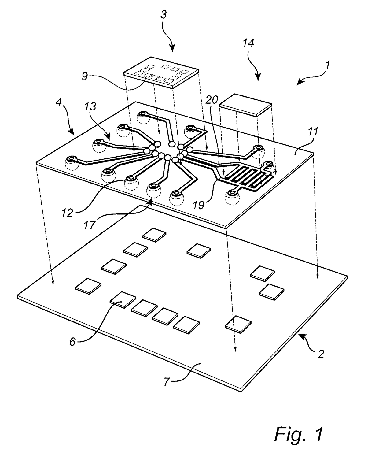
[0047]FIG. 1 schematically illustrates an electronic assembly 1 comprising a device substrate, here in the form of a simplified printed circuit board (PCB) 2, an integrated circuit (IC) 3, and an energy storing interposer device 4 according to an example embodiment of the present invention.

[0048]The PCB inc...


PUM


Abstract

An interposer device comprising an interposer substrate; a plurality of conducting vias extending through the interposer substrate; a conductor pattern on the interposer substrate, and a nanostructure energy storage device. The nanostructure energy storage device comprises at least a first plurality of conductive nanostructures formed on the interposer substrate; a conduction controlling material embedding each nanostructure in the first plurality of conductive nanostructures; a first electrode connected to each nanostructure in the first plurality of nanostructures; and a second electrode separated from each nanostructure in the first plurality of nanostructures by the conduction controlling material, wherein the first electrode and the second electrode are configured to allow electrical connection of the nanostructure energy storage device to the integrated circuit.

Description

FIELD OF THE INVENTION[0001]The present invention relates to an interposer device for arrangement between an electronic device and a device substrate to interconnect the first electronic device and the device substrate through said interposer device. The present invention also relates to a method of manufacturing such an interposer device.BACKGROUND OF THE INVENTION[0002]Electronic devices need electrical energy to operate. In a portable electronic device, a battery is typically provided, and electrical energy is drawn from the battery to power integrated circuits comprised in the electronic device. Moreover, a number of driving factors that are continuously improving the system level performance including but not limited to smaller form-factor with higher data transfer rate, signal integrity, memory bandwidth, power and thermal management capability etc. It is of highest importance that the today's integrated and portable products are continuously striving to improve at least those...

Claims


Application Information

Patent Timeline
IPC IPC(8): H01L23/498H01L21/48H01L23/14H01L23/538
CPCH01L23/49827H01L21/486H01L23/147H01L23/5389H01L23/50H01L23/49811H01G4/35H01L23/481H01L23/485H01L24/97
Inventor KABIR, M SHAFIQULJOHANSSON, ANDERSAMIN SALEEM, MUHAMMADENOKSSON, PETERDESMARIS, VINCENTANDERSSON, RICKARD
Owner SMOLTEK AB
Why Eureka
Try Eureka