Ceramic electronic device and manufacturing method of ceramic electronic device

Active Publication Date: 2019-06-13
TAIYO YUDEN KK
View PDF2 Cites 7 Cited by
  • Summary
  • Abstract
  • Description
  • Claims
  • Application Information

AI Technical Summary

Benefits of technology

[0008]According to another aspect of the present invention, there is provided a manufacturing method of a ceramic electronic device including: forming a ceramic multilayer structure having a parallelepiped shape, by stacking a plurality of pattern-formed sheets in each of which a conductive paste for forming internal electrode layers is printed on a part of a dielectric green sheet including ceramic, a margin paste including ceramic is printed on another part of the dielectric green sheet where the conductive paste for forming internal electrode layers is not printed, each of a plurality of conductive pastes for forming internal electrode layers being alternately exposed to two edge faces of the ceramic multilayer structure, and by providing cover sheets on an upper face and a lower face of the ceramic multilayer structure in a stacking direction of the ceramic multilayer structure; coating a conductive paste for forming external electrod

Problems solved by technology

In this case, a crack may occur in a part of a dielectric body under an external electrode in a corner portion (edge part), after the firing.
However, whe

Method used


Image

  • Ceramic electronic device and manufacturing method of ceramic electronic device
  • Ceramic electronic device and manufacturing method of ceramic electronic device
  • Ceramic electronic device and manufacturing method of ceramic electronic device

Examples


embodiment

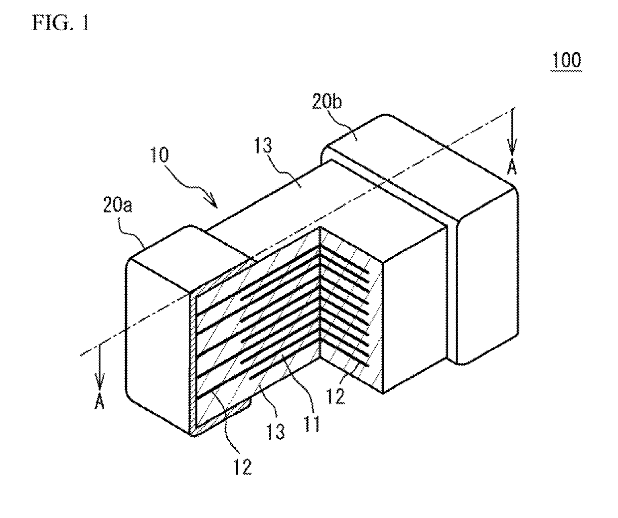
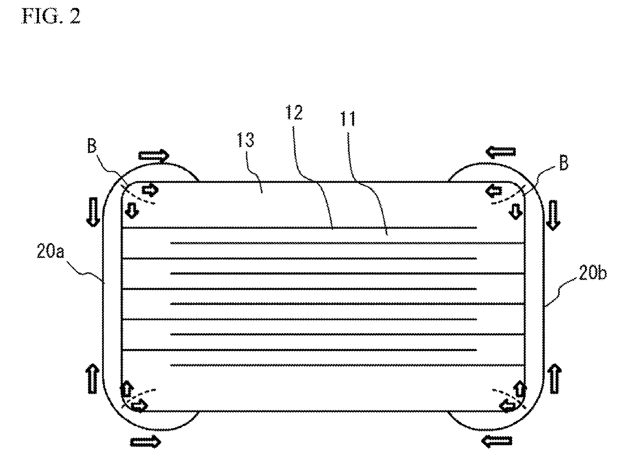
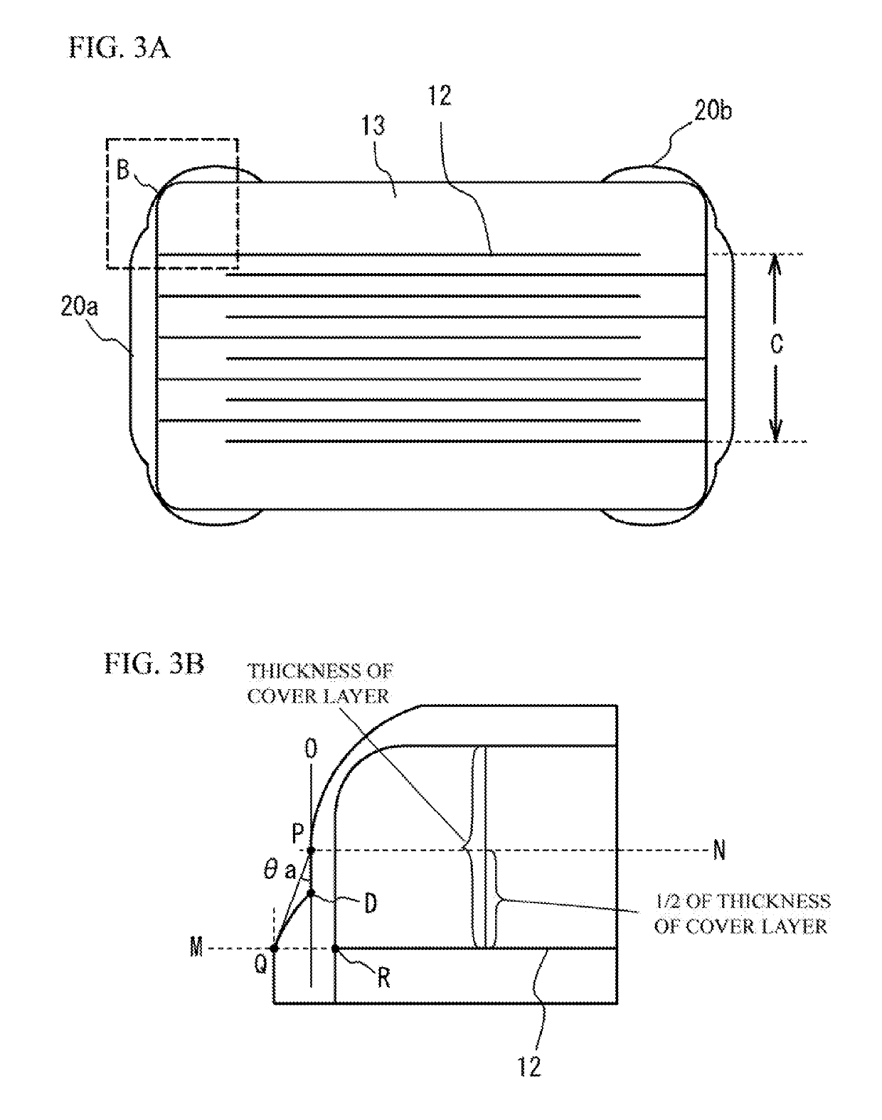
[0017]A description will be given of a multilayer ceramic capacitor. FIG. 1 illustrates a partial perspective view of a multilayer ceramic capacitor 100 in accordance with an embodiment. As illustrated in FIG. 1, the multilayer ceramic capacitor 100 includes a multilayer chip 10 having a rectangular parallelepiped shape, and a pair of external electrodes 20a and 20b that are respectively provided at two edge faces of the multilayer chip 10 facing each other. An upper face of the multilayer chip 10 in a stacking direction is referred to as an upper face. A lower face of the multilayer chip 10 in the stacking direction is referred to as a lower face. Two faces other than the two edge faces, the upper face and the lower face of the multilayer chip 10 are referred to as side faces. The external electrodes 20a and 20b extend to the upper face, the lower face and the two side faces. However, the external electrodes 20a and 20b are spaced from each other on the upper face, the lower face a...

examples

[0046]The multilayer ceramic capacitors in accordance with the embodiment were made and the property was measured.

examples 1 to 10

[0047]Necessary additive was added to barium titanate powders. The resulting powders were sufficiently wet-blended by a ball mil and were crushed. Thus, the dielectric material was obtained. An organic binder and a solvent were added to the dielectric material. And dielectric green sheets were made by a doctor blade method. The organic binder was polyvinyl butyral (PVB) resin or the like. The solvent was ethanol, toluene or the like. And a plasticizer and so on were added.

[0048]Next, the conductive paste for forming the internal electrode layer was formed. The conductive paste included a main component metal (Ni) powder of the internal electrode layer 12, a co-material (barium titanate), a binder (ethyl cellulose), a solvent and an auxiliary as needed.

[0049]The conductive paste for forming the internal electrode layer was screen-printed on the dielectric green sheet. The margin paste including the dielectric material was printed on the dielectric green sheet where the conductive pas...


PUM

PropertyMeasurementUnit
Angleaaaaaaaaaa
Angleaaaaaaaaaa
Thicknessaaaaaaaaaa

Abstract

A ceramic electronic device includes: a multilayer chip including a multilayer structure and cover layers, the multilayer structure having a structure in which each of a plurality of dielectric layers and each of a plurality of internal electrode layers are alternately stacked and are alternately exposed to two edge faces of the multilayer chip, a main component of the plurality of dielectric layers being a ceramic, the cover layers being provided on an upper face and a lower face of the multilayer structure in a stacking direction; and a pair of external electrodes that are formed on the two edge faces, wherein each of the external electrodes has a smaller thickness on a corner portion of the cover layers, has a crook toward the internal electrode layers, and has a larger thickness on an area of the two edge faces where the internal electrode layers are extracted.

Description

CROSS-REFERENCE TO RELATED APPLICATION[0001]This application is based upon and claims the benefit of priority of the prior Japanese Patent Application No. 2017-235726, filed on Dec. 8, 2017, the entire contents of which are incorporated herein by reference.FIELD[0002]A certain aspect of the present invention relates to a ceramic electronic device and a manufacturing method of a ceramic electronic device.BACKGROUND[0003]A ceramic electronic device such as a multilayer ceramic capacitor has a multilayer chip in which a plurality of dielectric layers of which a main component is ceramic and a plurality of internal electrode layers are alternately stacked. The internal electrode layers are extracted to an edge face of the multilayer chip. An external electrode covers the surface of the edge face. For example, sheets for the multilayer chip and a paste for the external electrode are fired together with each other (for example, see Japanese Patent Application Publication No. 2005-44903).S...

Claims


Application Information

Patent Timeline
IPC IPC(8): H01G4/248H01G4/30H01G4/012H01G4/232H01G4/008
CPCH01G4/248H01G4/30H01G4/012H01G4/2325H01G4/0085H01G4/1227H01G4/232H01G4/224
Inventor TAHARA, MIKIONAKAMURA, TOMOAKI
Owner TAIYO YUDEN KK
Why Eureka
Try Eureka