Shift register circuit and display panel

a register circuit and display panel technology, applied in electronic switching, digital storage, instruments, etc., can solve the problems of abnormal output signal and increase in power consumption, and achieve the effect of low cost and simple structur

Active Publication Date: 2019-08-15
TRIVALE TECH
View PDF0 Cites 14 Cited by
  • Summary
  • Abstract
  • Description
  • Claims
  • Application Information

AI Technical Summary

Benefits of technology

[0010]In the shift register circuit according to the present invention, at least one transistor included in the unit shift register includes a back gate electrode, and the back gate voltage generation circuit changes the voltage of the back gate electrode according to the voltage of the gate electrode of the transistor. This makes it possible to compensate for the shift of the threshold voltage of the transistor in the reverse direction and stably turn on and off the transistor at an appropriate timing. Furthermore, since the back gate voltage generation circuit is driven by using the power supply originally used by the unit shift register, it is unnecessary to add a power supply for the back gate voltage generation circuit. Therefore, it is possible to change the voltage of the back gate electrode of the transistor with a simple structure and at a low cost.
[0011]The objects, features, aspects, and advantages of the present invention will become more apparent from the following detailed description and the accompanying drawings.

Problems solved by technology

This causes a malfunction such as an increase in power consumption and abnormality of the output signal.

Method used


Image

  • Shift register circuit and display panel
  • Shift register circuit and display panel
  • Shift register circuit and display panel

Examples


first embodiment

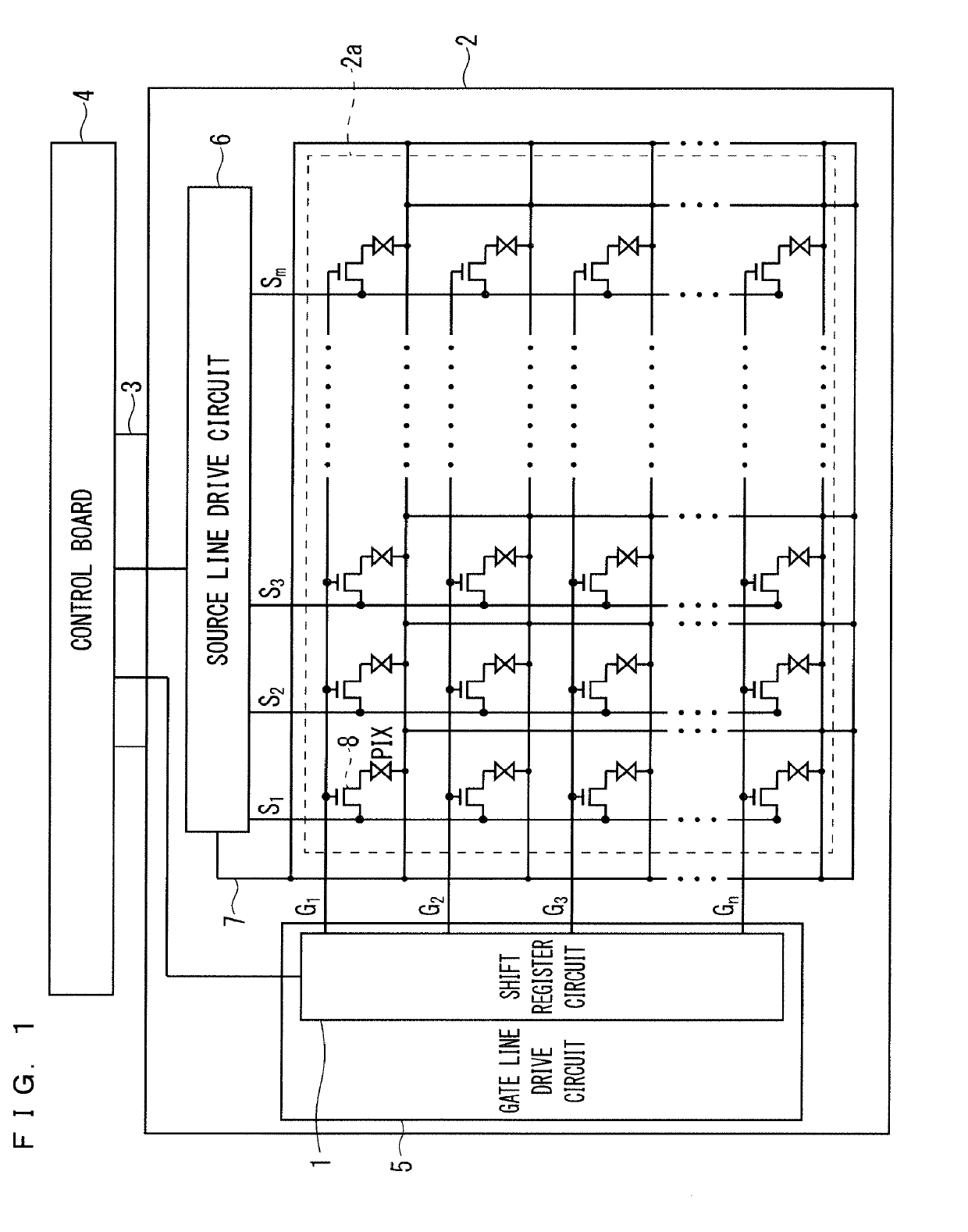
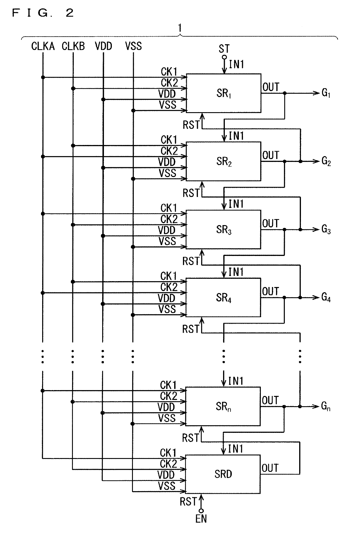
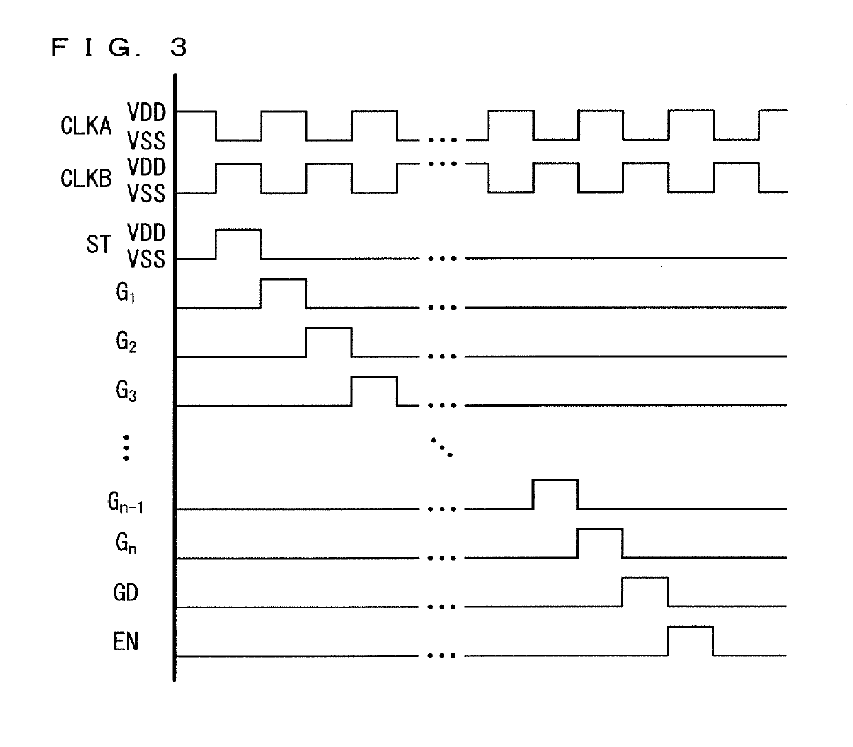
[0038]FIG. 1 is a diagram showing a configuration of a liquid crystal display device in the first embodiment. As shown in FIG. 1, the liquid crystal display device includes a display panel 2, a flexible printed circuit board 3, and a control board 4.

[0039]The display panel 2 is an active matrix display panel. The display panel 2 is an active matrix display panel in which a display region 2a, a plurality of gate lines (scanning signal lines), a plurality of source lines (data signal lines), a gate line drive circuit 5, and a source line drive circuit 6 are built by using amorphous silicon, an oxide semiconductor, or the like on a glass substrate.

[0040]In the display region 2a, a plurality of pixels PIX is arranged in a matrix. The pixel PIX includes a TFT 8 being a pixel selection element, a liquid crystal capacitor, and an auxiliary capacitor. The gate of the TFT8 is connected to a gate line, and the source of the TFT 8 is connected to a source line. The liquid crystal capacitor and...

second embodiment

[0122]In the unit shift register SR in the first embodiment, it is assumed that the first transistor Q1 and the back gate transistor Q5 are normally off in the initial state. On the other hand, in the unit shift register SR in the second embodiment, it is assumed that the back gate transistor Q5 is normally on from the initial state.

[0123]FIG. 10 is a diagram showing the characteristics of the drain-source current when the back gate transistor Q5 is normally off (first embodiment) and normally on (second embodiment). As shown in FIG. 10, when the back gate transistor Q5 is normally off, almost no drain-source current flows when the gate and the source are at the same potential. On the other hand, when the back gate transistor Q5 is normally on, a drain-source current flows even when the gate and the source are at the same potential.

[0124]In particular, it is known that, a TFT using an oxide semiconductor, because of deposition conditions and thermal history of an oxide semiconductor...

third embodiment

[0136]FIG. 15 is a diagram showing the configuration of the unit shift register SR in the third embodiment. In the back gate voltage generation circuits 300 and 300A (FIGS. 4 and 11) of the first and second embodiments, the case where the back gate node N2 is connected to only the back gate capacitor element C2 is described. On the other hand, the back gate voltage generation circuit 300B of the third embodiment further includes a voltage dividing capacitor element C3.

[0137]As shown in FIG. 15, the voltage dividing capacitor element C3 is connected between the back gate node N2 and the first power supply terminal S2 having the potential VSS. The back gate node N2 is connected between the back gate capacitor element C2 and the voltage dividing capacitor element C3.

[0138]In the third embodiment, since the configuration of the liquid crystal display device and the configuration of the shift register circuit 1 are the same as those of the first embodiment (FIGS. 1 and 2), the descriptio...


PUM


Abstract

A shift register circuit that controls back gate voltage of a transistor with a simple configuration and at a low cost, and a display panel. In the shift register circuit, shift registers include: an output circuit, a charge and discharge circuit, a first power supply terminal, and at least one back gate voltage generation circuit. The output circuit or the charge and discharge circuit includes at least one transistor. The back gate voltage generation circuit includes a back gate node. The back gate node is connected to the back gate electrode of the transistor. The back gate voltage generation circuit changes a voltage of the back gate node according to a voltage of a gate electrode of the transistor. The back gate voltage generation circuit is supplied with a drive voltage from the first power supply terminal.

Description

TECHNICAL FIELD[0001]The present invention relates to a shift register circuit and a display panel, and more particularly to a shift register circuit including a plurality of unit shift registers cascade-connected in multistage and a display panel.BACKGROUND ART[0002]In an image display device such as a liquid crystal display device, it is possible to use a shift register for performing a shift operation that makes a round in one frame period of the display signal as a gate line drive circuit (scanning line drive circuit) for scanning the display panel. In order for the number of steps in the manufacturing process of the display device to decrease, the shift register preferably includes only field effect transistors of the same conductivity type.[0003]The display device in which a shift register of a gate line driver circuit is constituted with a thin film transistor (hereinafter referred to as “TFT”) whose channel region is formed of an amorphous semiconductor is easily increased i...

Claims


Application Information

Patent Timeline
Patent Type & Authority Applications(United States)
IPC IPC(8): G09G3/36G11C19/18G11C19/28
CPCG09G3/3677G11C19/184G11C19/28G09G2300/0408G09G2310/0286G09G3/20G09G3/36H03K17/30G09G2310/0267G11C19/287
Inventor ONO, TAKESHIAGARI, MASAFUMIFUJINO, TOSHIAKIKAWABUCHI, SHINJI
Owner TRIVALE TECH
Why Eureka
Try Eureka