

Circuit board assembly inspection method
- Summary
- Abstract
- Description
- Claims
- Application Information
AI Technical Summary
Benefits of technology
Problems solved by technology
Method used
Image

Examples
Embodiment Construction
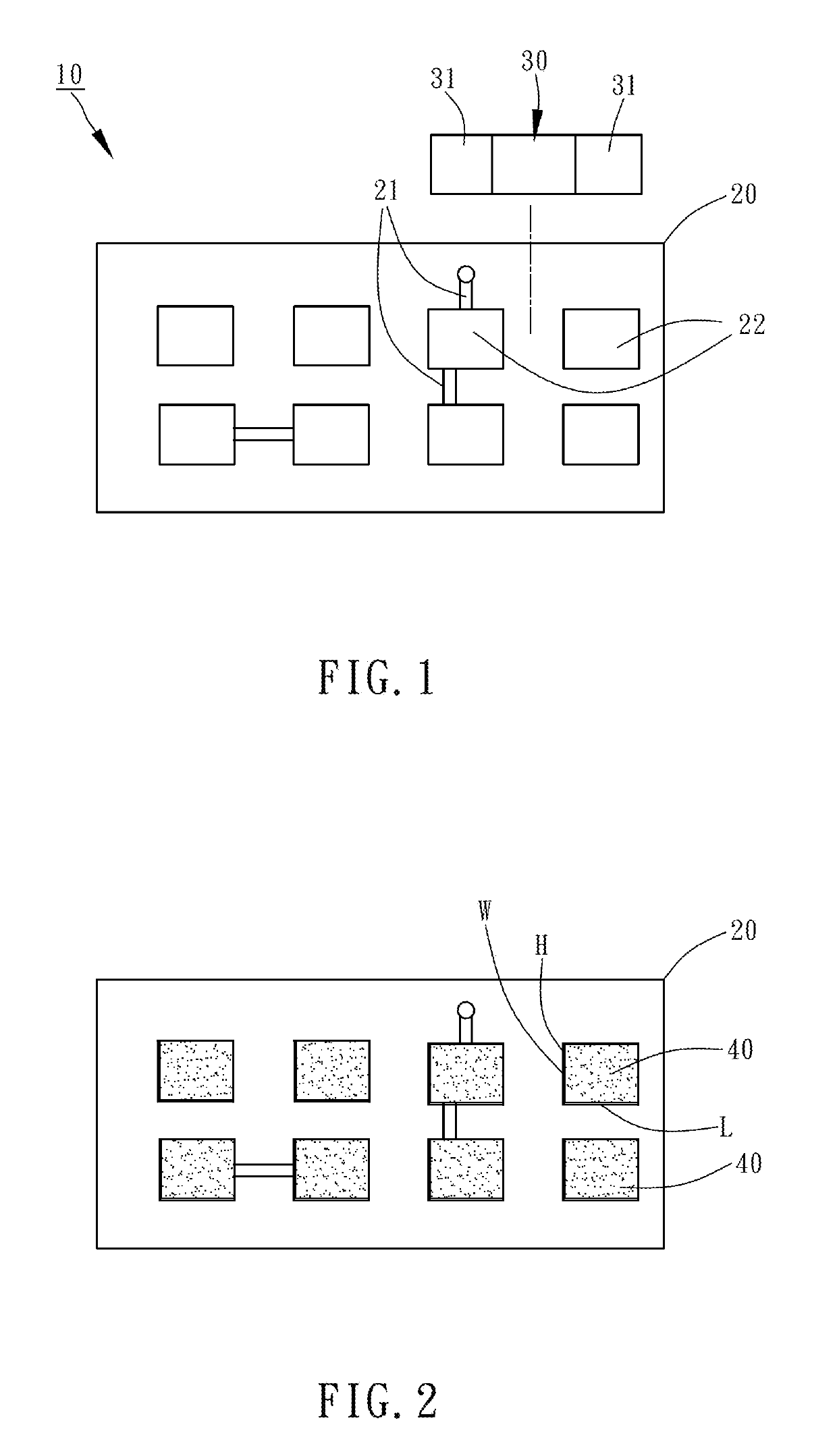
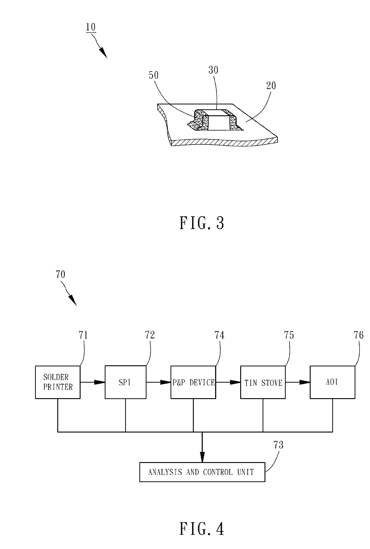
[0022]In the terms used in the following embodiments, “circuit board” refers to a printed circuit board (PCB), which is a carrier of electronic components but does not contain electronic components; “circuit board assembly” refers to a collection of both a circuit board and electronic components soldered to the circuit board; “solder layer” refers to a layer of solder disposed on a solderable area of the circuit board prior to soldering the electronic components to the circuit board, and the solder layer is usually a solder paste; “solder joint layer” refers to a connecting structure formed between the pins of the electronic component and the circuit board when the pins of the electronic component are soldered to the circuit board. The connecting structure is made from the solder layer. Thus the composition of the connecting structure is solder. The “solder joint layer” may also be referred to as “solder joint” or “soldering point,” but to prevent the term “solder joint” from being ...
PUM
| Property | Measurement | Unit |
|---|---|---|
| Length | aaaaa | aaaaa |
| Width | aaaaa | aaaaa |
Abstract
Description
Claims
Application Information