

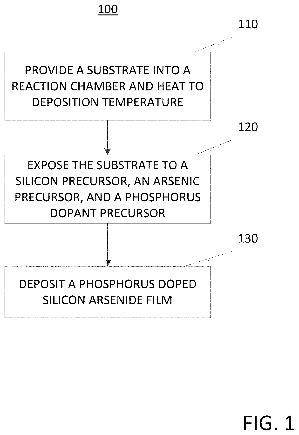
Method for depositing a phosphorus doped silicon arsenide film and related semiconductor device structures
a technology of phosphorus doped silicon and semiconductor devices, which is applied in the direction of crystal growth process, polycrystalline material growth, chemically reactive gas, etc., can solve the problems of deterioration of device performance, huge challenges for conventional device scaling, etc., and achieve the effect of preventing the diffusion of dopants
- Summary
- Abstract
- Description
- Claims
- Application Information
AI Technical Summary
Benefits of technology
Problems solved by technology
Method used
Image

Examples
Embodiment Construction
[0015]Although certain embodiments and examples are disclosed below, it will be understood by those in the art that the invention extends beyond the specifically disclosed embodiments and / or uses of the invention and obvious modifications and equivalents thereof. Thus, it is intended that the scope of the invention disclosed should not be limited by the particular disclosed embodiments described below.
[0016]As used herein, the term “substrate” may refer to any underlying material or materials that may be used, or upon which, a device, a circuit or a film may be formed.
[0017]As used herein, the term “phosphorus doped silicon arsenide” may refer to a material comprising both silicon species and arsenic species as well as active phosphorus dopant species.
[0018]As used herein, the term “film” and “thin film” may refer to any continuous or non-continuous structures and material deposited by the methods disclosed herein. For example, “film” and “thin film” could include 2D materials, nano...
PUM
| Property | Measurement | Unit |
|---|---|---|
| temperature | aaaaa | aaaaa |
| temperature | aaaaa | aaaaa |
| temperature | aaaaa | aaaaa |
Abstract
Description
Claims
Application Information