Dielectric waveguide line, connection structure and method for producing dielectric waveguide line

a dielectric waveguide and connection structure technology, applied in waveguides, electrical devices, coupling devices, etc., can solve problems such as loss of transmission efficiency, and achieve the effects of reducing rapid change of impedance, reducing permittivity, and being easy to connect to each other

Active Publication Date: 2020-01-30
DAIKIN IND LTD +1
View PDF0 Cites 0 Cited by
  • Summary
  • Abstract
  • Description
  • Claims
  • Application Information

AI Technical Summary

Benefits of technology

[0029]The first dielectric waveguide of the invention may be connected to a hollow metallic tube for use. The connection of the dielectric waveguide to the hollow metallic tube can be achieved by inserting the dielectric waveguide into the hollow metallic tube. Thus, the hollow metallic tube and the dielectric waveguide can be easily connected to each other. The dielectric waveguide includes a dielectric waveguide body and a dielectric waveguide end having a lower permittivity than the dielectric waveguide body. This can reduce a rapid change in impedance between the dielectric waveguide and the hollow metallic tube and enables a connection structure exhibiting low transmission and return losses. The dielectric waveguide body and the dielectric waveguide end are seamlessly and monolithically formed from the same material. This can eliminate the need for processing to form an interface and lead to excellent transmission efficiency. Accordingly, a change in impedance at an interface does not occur even when the dielectric waveguide is bent and a stress is applied. Thus, the dielectric waveguide can exhibit stable properties even when bent.
[0030]The second dielectric waveguide of the invention may be connected to a hollow metallic tube for use. The connection of the dielectric waveguide to the hollow metallic tube can be achieved by inserting the dielectric waveguide into the hollow metallic tube. Thus, the hollow metallic tube and the dielectric waveguide can be easily connected to each other. The dielectric waveguide includes a dielectric waveguide body and a dielectric waveguide end having a lower density than the dielectric waveguide body. This can reduce a rapid change in impedance between the dielectric waveguide and the hollow metallic tube and enables a connection structure exhibiting low transmission and return losses. The dielectric waveguide body and the dielectric waveguide end are seamlessly and monolithically formed from the same material. This can eliminate the need for processing to form an interface and lead to excellent transmission efficiency. Accordingly, a change in impedance at an interface does not occur even when the dielectric waveguide is bent and a stress is applied. Thus, the dielectric waveguide can exhibit stable properties even when bent.
[0031]The connection structure of the invention can provide a connection between a hollow metallic tube and a dielectric waveguide by insertion of the dielectric waveguide into the hollow metallic tube. Thus, the hollow metallic tube and the dielectric waveguide can be easily connected to each other. The dielectric waveguide includes a dielectric waveguide body and a dielectric waveguide end having a lower permittivity or density than the dielectric waveguide body. This can reduce a rapid change in impedance between the dielectric waveguide and the hollow metallic tube and enables low transmission and return losses. The dielectric waveguide body and the dielectric waveguide end are seamlessly and monolithically formed from the same material. This can eliminate the need for processing to form an interface and lead to excellent transmission efficiency.
[0032]The production method of the invention having the above features enable easy production of a dielectric waveguide that includes a dielectric waveguide end having a lower permittivity or density than a dielectric waveguide body, that is easily processed and connected even when having a small diameter, and that can provide a connection structure exhibiting low transmission and return losses of high frequency signals.

Problems solved by technology

A rapid change in impedance may cause reflection of high frequency signals, resulting in loss of transmission efficiency.

Method used


Image

  • Dielectric waveguide line, connection structure and method for producing dielectric waveguide line
  • Dielectric waveguide line, connection structure and method for producing dielectric waveguide line
  • Dielectric waveguide line, connection structure and method for producing dielectric waveguide line

Examples


examples

[0126]The invention is described with reference to examples. These examples are not intended to limit the invention.

experimental example

[0127]PTFE fine powder (SSG: 2.175) in an amount of 100 parts by mass was mixed with 20.5 parts by mass of Isopar G available from Exxon Mobil Corp. serving as an extrusion aid, and the mixture was aged at room temperature for 12 hours. Thereby, extrusion aid-mixed powder was obtained. This extrusion aid-mixed powder was put into a pre-molding machine and pressurized at 3 MPa for 30 minutes. Thereby, a cylindrical pre-molded article was obtained.

[0128]This pre-molded article was paste-extruded using a paste extruder, and then heated at 200° C. for one hour so that the extrusion aid was evaporated. Thereby, a resin line having a diameter of 3.51 mm was obtained.

[0129]This resin line was cut so as to have a total length of 660 mm.

Outer layer:

[0130]PTFE fine powder was mixed with Isopar G available from Exxon Mobil Corp. serving as an extrusion aid, and the mixture was aged at room temperature for 12 hours. Thereby, extrusion aid-mixed powder was obtained. This extrusion aid-mixed powd...

example 1

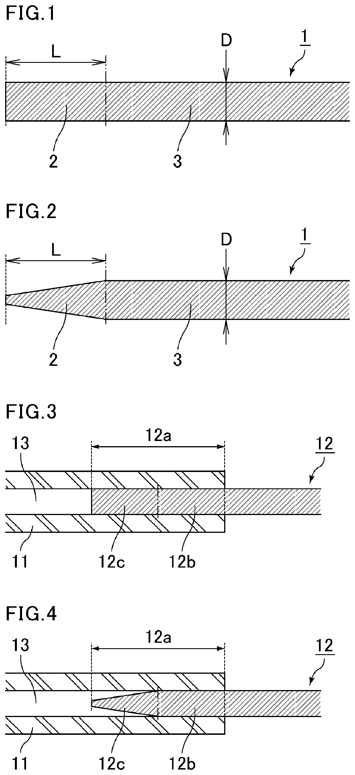
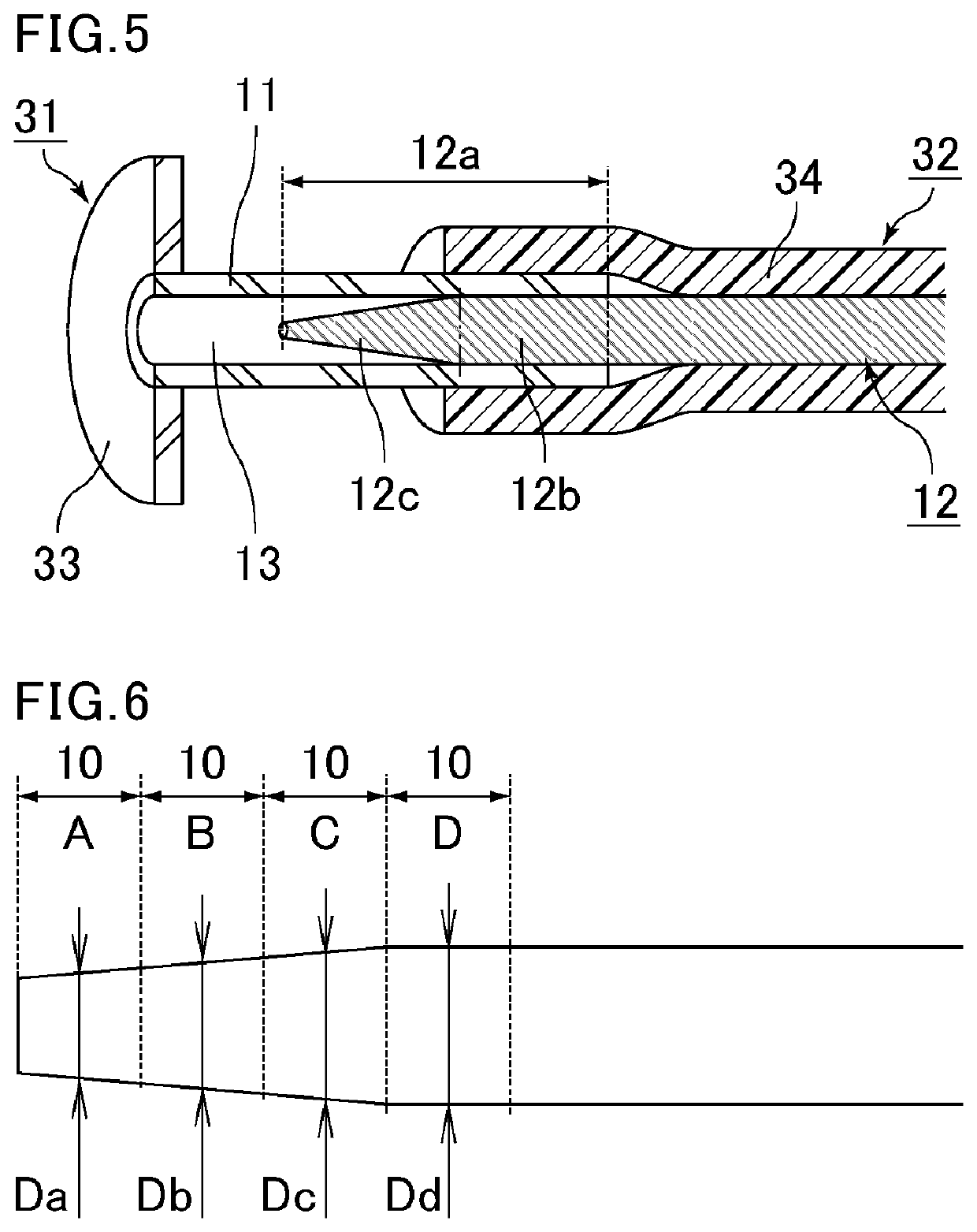
[0133]The resin line obtained in the experimental example was heated at 330° C. for 70 minutes. A portion (end) 20 mm or less apart from a tip of the resin line was heated at 260° C. A portion 5 mm or less apart from the tip was then held and the end was stretched at a stretch ratio of two times and at a stretching speed of 200% / sec in the longitudinal direction. Thereby, the end was stretched to 40 mm. After the stretching, a portion 10 mm or less apart from the tip held in the stretching was cut off. Thereby, a dielectric waveguide was obtained.

[0134]This dielectric waveguide was inserted into the outer layer obtained in the experimental example. Thereby, a dielectric waveguide including an outer layer was obtained.


PUM

PropertyMeasurementUnit
densityaaaaaaaaaa
densityaaaaaaaaaa
temperatureaaaaaaaaaa

Abstract

The invention provides a dielectric waveguide for transmitting millimeter waves or sub-millimeter waves. The dielectric waveguide is easily processed and connected even when having a small diameter, and can provide a connection structure exhibiting low transmission and return losses of high frequency signals. The dielectric waveguide includes a dielectric waveguide body and a dielectric waveguide end having a lower permittivity than the dielectric waveguide body. The dielectric waveguide body and the dielectric waveguide end are seamlessly and monolithically formed from the same material.

Description

TECHNICAL FIELD[0001]The invention relates to dielectric waveguides, connection structures, and methods for producing a dielectric waveguide.BACKGROUND ART[0002]Dielectric waveguides, waveguides, coaxial cables, and similar devices are used to transmit high frequency signals such as microwaves and millimeter waves. In particular, dielectric waveguides and waveguides are used as transmission lines for high frequency band electromagnetic waves such as millimeter waves. A common dielectric waveguide is composed of an inner layer and an outer layer and it utilizes the difference in permittivity between the layers to transmit electromagnetic waves by side reflection. The outer layer may be the air. Still, in order to stabilize the permittivity and to achieve easy handling, the outer layer is usually a soft structure made of, for example, resin foam having low tan δ and low permittivity. In practical implementation, transmission lines of different kinds are often coupled with each other. ...

Claims


Application Information

Patent Timeline
Patent Type & Authority Applications(United States)
IPC IPC(8): H01P3/16H01P5/08H01P11/00
CPCH01P11/006H01P3/16H01P5/087
Inventor YOSHIMOTO, HIROYUKIFUKAMI, DAIYAMANAKA, TAKUHORIBE, MASAHIROKATO, YUTOSAKAMAKI, RYO
Owner DAIKIN IND LTD
Why Eureka
Try Eureka